In a time when much of the success and profitability of next-generation products rests on time-to-market (TTM), taking designs from concept to high-resolution, fully functional prototypes has become an increasingly critical component of the new product introduction process. And in the brutally competitive electronics market, the 3D/Additive Manufacturing (AM) process of Stereolithography or SLA is proving especially attractive in saving time and resources, keeping risks and costs as low as possible. While around for several decades as a means of producing prototypes, designers are now also prospecting the idea of fully functional components using SLA, as AM processes become sophisticated to the point of allowing the production of complex, embedded electronics prototypes.
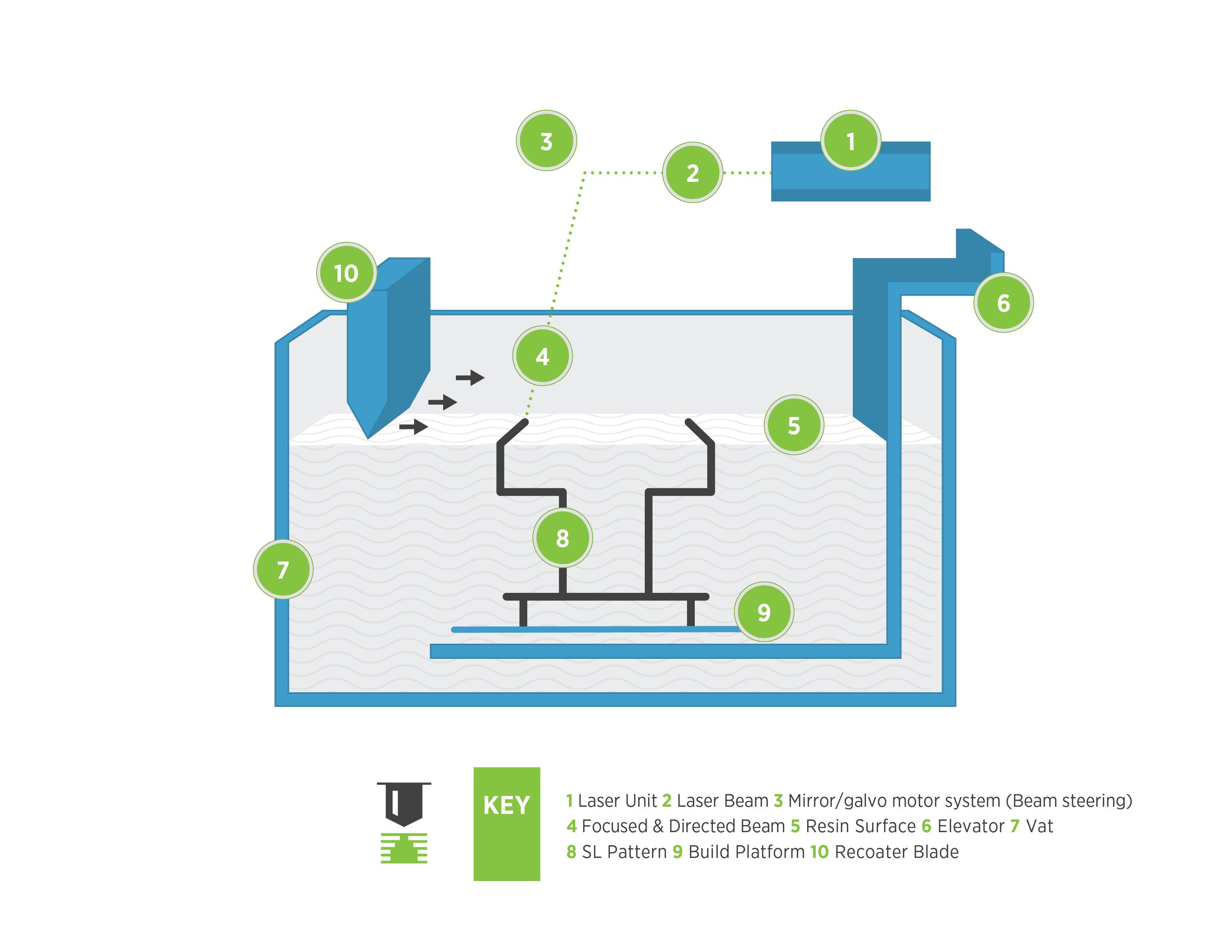
Stereolithography represents much of the rapid prototyping systems currently in place and no doubt contributes significantly to overcoming the challenge of getting to the market first with quality products and lower production costs. This Additive Manufacturing process begins with a 3D CAD model that is broken into a finite-element model. That model is the blueprint behind a computer-controlled ultraviolet laser that focuses on a small point to draw on the surface of UV-curable liquid thermoset resin. Where it draws, the liquid turns to solid. The process is repeated in thin two-dimensional cross sections with the first part layer adhering to each additional layer to form complex, 3D parts. The process is relatively quick and produces accurate parts without machining, cutting, or employ tools such molds, patterns, jigs, fixtures — all of which can add significant costs. And all this in a matter of hours.
The capability of speeding up the prototyping process to under two days or even hours makes SLA especially attractive for designers in the competitive electronics market. While in that first stage of product development – creating a proof of concept prototype — specs and requirements often change even as your prototype supplier has begun work on your project. A two-day or less window, as opposed to weeks, gives you the flexibility to work through any potential design flaws or defects without costly redo’s while in prototype and, more importantly, before the manufacturing process. This also becomes increasingly important when creating low volume products with complex design and geometrical configurations — an added advantage with SLA.
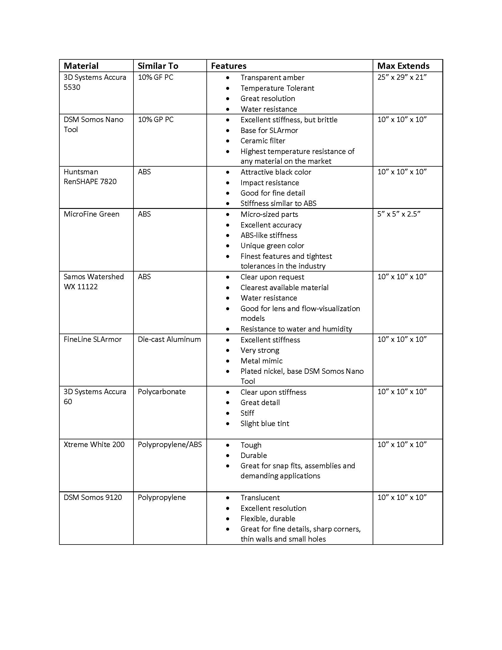
Materials key to additive manufacturing process
SL provides the widest selection of material, best feature resolution, and smoothest surface finish. It works well for very small parts and complex geometries during early prototyping. Below are the materials that Proto Labs for 3D printing.


Leave a Reply
You must be logged in to post a comment.