Clock Jitter is commonly used to describe the performance requirements of oscillators and PLLs when driving high performance components like FPGAs, Microprocessors, and PHYs. But the plethora of clock jitter types, measurement methodologies, and corresponding specifications is broad and often leads to confusion. It is important to use the jitter type that is most appropriate for the application of interest. The purpose of this document is to provide some basic guidelines for selecting and quantifying the relevant jitter specification for a given application, as summarized in Table 1.

Frequency domain jitter
According to Fourier, any periodic wave (i.e. clock signal) can be constructed as an infinite sum of a series of Sine Waves, as shown in Figure 1. Thus, a clock signal can be described as a set of frequencies and corresponding amplitudes. The nominal frequency of a clock is called the Fundamental (also called F0, or the 1st harmonic). Integer multiples of F0 are called the Harmonics. The “Perfect Clock” is built with only odd Harmonics, in ever decreasing amplitude.

No real world clock signal is perfect, however. Sideband spectral content on the Fundamental implies frequency deviation, or timing jitter, which is what clock jitter specifications attempt to quantify. Note that there is both positive and negative sideband content, which is characteristic of random jitter. The Phase Noise (PN) of a clock signal, represented as a PN Plot as shown in Figure 2, is a quantification of this Fundamental sideband content. Typically generated by Spectrum Analyzer test equipment, a PN Plot is particularly useful for seeing the frequency characteristics contributions of clock jitter that would otherwise take very long sample times and long record lengths to measure in the time domain.

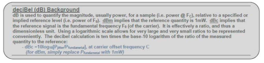
The term Phase Noise is not to be confused with Phase Jitter (or, Accumulated Jitter). Phase Noise is the term most commonly used to describe the “randomness” quality of instantaneous phase fluctuations. The corresponding frequency fluctuation, and thus period fluctuation, is a function of these instantaneous phase fluctuations. Thus, a PN Plot is a frequency domain representation of clock jitter, and is effectively the magnitude of jitter at the specific frequency deviation points from the mean. And, the magnitude (or power) of the jitter at a particular frequency deviation is a function of how often that deviation occurs. So, in summary, a PN Plot is effectively an indication of how often a particular period deviation occurs. And, the lower the dBc value for a given carrier offset frequency, the better.
The term RMS Phase Jitter is used to denote that the RMS Jitter value that is extrapolated from a frequency domain Phase Noise Plot. The terminology is intended to differentiate this jitter type from “RMS Jitter” previously detailed in this paper, which is strictly a time domain measurement of Period Jitter. As detailed by Parseval’s Theorem, the conversion to an RMS Phase Jitter value from a PN Plot is largely an integral function (i.e. area under the PN Plot). For this reason, the integration range for RMS Phase Jitter is a necessary qualifier for this specification. This integration range is also referred to as the “mask”, and is effectively the jitter frequency filter specific to the application. The purpose of this jitter mask is to restrict the quantification of jitter to the range of jitter frequencies that are not filtered by the application transfer function. The quantification of jitter in the frequency domain, represented by an RMS Phase Jitter specification, makes this clock jitter type particularly relevant for SerDes use cases (i.e. SDH, SONET, Ethernet, XAUI, PCIe, sRIO), as shown in Figure 3.
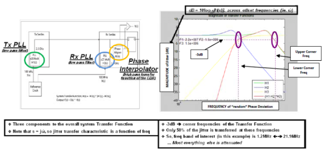
The Phase Interpolator is part of the Rx SerDes CDR circuitry and its transfer function is effectively a high pass filter (H3). But the Tx SerDes PLL (H1) and the Rx SerDes PLL (H2) transfer functions are effectively low pass filters that attenuate high frequency noise present on their respective inputs. And, the total transfer function of the system is given by: Ht(s) = [H1(s)-H2(s)]*H3(s).
A very important benchmark for a given PLL is its bandwidth, also referred to as its “-3dB corner frequency”. This is effectively the nominal frequency offset at which only 1⁄2 the power of the input clock jitter is transferred to the output. Note that the composite SerDes transfer function is comprised of both an upper -3dB corner frequency and a lower – 3dB corner frequency. And, clock jitter outside these corner frequencies is effectively attenuated.
The origin of the upper and lower corner frequencies for a SerDes transfer function is further detailed in Figure 4. The Tx SerDes Clock Multiplying PLL acts as a low pass filter. As a result, high frequency jitter present on the Tx Refclk is not transferred to the output of that PLL. This effectively defines the upper -3dB corner frequency of the integration band of interest.

Similarly, the Rx SerDes CDR complex on the receiving end of a serial data link used to recover the in-band clock also uses an internal PLL, and thus will also only pass the low frequency jitter on the Refclk. This is what effectively defines the lower -3dB corner frequency for the integration band of interest. Typically, both the Tx PLL and the Rx PLL track low frequency jitter and attenuate high frequency jitter. So, it is the mid-range frequencies of most interest since the PLLs do not necessarily track these equally. Together, these effects bound the SerDes Transfer Function for the given application. If the RMS Phase Jitter is too high for the integration band of interest, then FIFO over/under-runs will increase beyond an acceptable error rate for the given application.
Thus, the RMS Phase Jitter requirements for a clock used to drive a SerDes must be qualified with the application specific jitter mask, or filter. Some example application specific filters include:
• Fibre Channel (637 KHz <<>> 10 MHz)
• 10 Gigabit Ethernet XAUI (1.875 MHz <<>> 20 MHz) • SONET OC-48 (12 KHz <<>> 20MHz)
• SONET OC-192 (20 KHz <<>> 80MHz)
• SATA/SAS (900 KHz <<>> 7.5 MHz)
The various network communications standards (i.e. GE, 10GE, etc.) often specify Pk-Pk Total Jitter Unit Interval (UI) as a percentage of 1 UI. This is actually a SerDes eye closure specification that must be met in order to meet the acceptable BER, which is typically 10-12 for many of the standards. This specification is still bounded by an integration range of interest. But, a Pk-Pk Total Jitter UI specification requires conversion to a corresponding random jitter specification in order that one may quantify the required “random” RMS Phase Jitter value. Here are some common system level jitter budget assumptions that may be applied in order to arrive at a jitter budget for the clock driving the SerDes.
- A typical Pk-Pk Total Jitter (TJ) limit is 0.65 UI (bit errors occur when the eye is only 35% open)
- Random Jitter (RJ) is budgeted 1⁄4 the Total Jitter
- Most of the RJ comes from the clock and SerDes
- But, conservatively assume the clock is budgeted 1⁄4 the RJ budge
- 10-12 BER is most common, so remember 14 as the number of standard deviations
- Divide TJpk-pk (0.65 * 1 UI) by 224 (14*4*4) to get the acceptable random RMS Phase Jitter.
- If not specified, then;
– For long range communication, use a 12 KHz – 20MHz filter
– For short range communication, divide baud rate by 1667 to get lower -3dB corner frequencY
For example, consider 10 Gigabit Ethernet implemented as four XAUI SerDes lanes each running 3.125Gbps. The corresponding RMS Phase Jitter requirement is calculated as follows.
- One UI for 3.125Gbps = 320pS
- Pk-Pk Total Jitter = (0.65 * 320pS) = 208pS
- 10 GE specifies a jitter mask from 1.875MHz -to- 20MHz
- Thus, the “random” RMS Phase Jitter = (208pS)/224 = 930fs (1.875MHz <> 20MHz)
It is important to note that the acceptable magnitude of RMS Phase Jitter, and the integration band of interest, is often dictated by the PHY vendor’s Refclock jitter specifications. And, the Refclock specifications from the PHY vendors often differ slightly from the industry standard and the application assumptions used in this section.
Phase Noise and RMS Phase Jitter are also relevant for RF Signal Chain design. Consider the use case of a high performance ADC in the signal chain path. Typically, ADC architectures implement a sample-and-hold (S&H) circuit that takes a snapshot of the ADC input at an instant in time, as shown in Figure 5.

When the S&H switch is closed, the network at the input of the ADC is connected to the sample capacitor. At the instant the switch is opened, one half-clock period later, the voltage on the capacitor is recorded and held. Variation in the time at which the switch is opened is known as aperture uncertainty (i.e. jitter), and will result in an error voltage that is proportional to the magnitude of the sampling clock jitter and the sampled analog input signal slew rate. RMS Phase Jitter on the sampling clock is convenient expression of this jitter as it yields a single number useful for calculation of ADC SNR degradation due to aperture jitter. But, a detailed look at the actual spectral content in a PN Plot can be more instructive. Elevated wideband noise may not produce a poor RMS Phase Jitter result, but will degrade SNR. Close-in phase noise causes the fundamental signal to spread into adjacent frequency bins of an FFT, thereby reducing dynamic range. Broadband phase noise will uniformly elevate the noise floor throughout the Nyquist zone thus reducing the overall ADC SNR performance.
IDT includes PN Plots and corresponding RMS Phase Jitter specifications in the datasheets of high performance PLL devices targeted for wired (i.e. SerDes) and wireless (i.e. RF Signal Chain) communications applications. As an example, consider the PN Plot and the corresponding RMS Phase Jitter measurement from the device datasheet of the IDT 8T49N282 Universal Frequency Translator, shown below. Note that the carrier frequency and integration range need to be specified for the quoted RMS Phase Jitter. With these qualifiers, the RMS Phase Jitter for a 156.25MHz carrier, integrated from 12 KHz <<>> 20 MHz, is measured to be ~ 314fs for this device.

A PN Plot is primarily intended to be a representation of random clock jitter. But, there are actually two main classifications of jitter; random jitter, and deterministic jitter. Random jitter is what is represented by the characteristic curve of the PN Plot, and is the primary measure of PLL jitter quality. But, real world applications always have some amount of deterministic jitter. And, this deterministic jitter can be quantified by the corresponding Spurs that show up in the PN Plot. For instance, the 8T49N282 example PN Plot (above) exhibits a -127dBc Spur centered at ~3.8 MHz offset frequency and another -122dBc Spur centered at ~7.6MHz offset frequency.
It is worth noting that it is not always easy to root cause the source of spurious content. Spurs can manifest themselves as second and third order sums and/or differences of different frequencies generated from within and/or outside the PLL device. Often times, the only way to root cause spurious content is to turn off (or modify) one at a time each potential modulation source and note any corresponding changes in the PN Plot.
Deterministic jitter is always bounded in amplitude and has a very specific (non-random) root cause. The potential sources of deterministic spurious content can be the PCB design itself, including;
• Crosstalk – The incremental inductance of a current carrying PCB trace will induce a magnetic field that can then impact a nearby parallel trace. This nearby trace will convert this magnetic field to an induced current superimposed on its otherwise typical drive characteristic. This induced current will affect the corresponding voltage, which will manifest itself as a deterministic jitter source that shows up as a Spur on a PN Plot. Component placement and PCB routing are important considerations for alleviating this type deterministic jitter
• EMI – RF Signal sources and AC power lines are examples of sources of Electromagnetic Interference (EMI). EMI sources can induce a noise current on a clock signal path. This phenomena and considerations are similar to that detailed for crosstalk.
• Power Supply Switcher – Often times Spurs seen on the PN Plot of a PLL output can be traced to the switching frequency of a Synchronous Buck Switching Regulator used as power source for the same PLL. Spurs will often show up at an offset frequency equal to the switcher frequency, and/or its harmonics. Understanding the frequency characteristic of the power supply switcher can be useful for designing a corresponding power supply filter circuit.
Consider the PN Plot of IDT’s 8413S12 used with a noisy power supply, as shown in Figure 6.
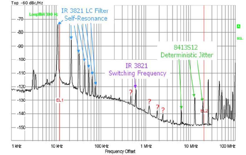
This design has significant spurious content observed at the output of the PLL. Root cause analysis made use of an EMI sniffer to trace back the Spurs to the Synchronous Buck Switching Regulator used in this design. Several layout modifications were implemented in order to reduce amount of noise that the 8413S12 picked-up from the regulator. Additional PCB design modifications were also implemented;
• The 11 KHz Spur, and its harmonics, is due to the regulator’s L-C filter circuit. This Spur was moved to 1 KHz offset with simple passive component changes to the L-C filter, placing the Spur outside the 12KHz <<> 20MHz integration range of interest.
• The 600 KHz Spur, and its harmonics, is a direct result of the regulator’s switching frequency of ~600kHz. This Spur was alleviated by adding an additional 100μF cap to the power supply filter circuit at the PLL’s analog power pin.
However, some of the spurious content comes from the 8413S12 device itself, as is also shown in Figure 6. Any clock synthesizer device with multiple outputs providing different frequencies can create undesirable sum and/or difference beat frequencies, which may be significant enough to show up as a Spur on a PN Plot. Also, the PLL architecture itself may explain some of the spurious content. Consider a simple Integer PLL architecture, as shown in Figure 7.
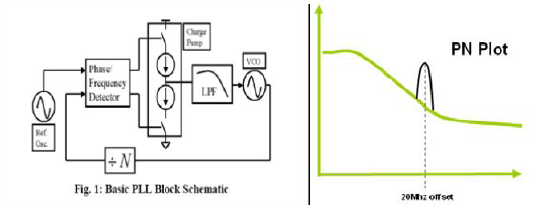
The Phase Detector (PD) and the Charge Pump deliver +/- pulses to the Loop Filter, which integrates these pulses to generate the tuning voltage for the Voltage Controlled Oscillator (VCO). But, even when the PLL is locked, the Charge Pump still outputs small charges due to mismatches in PLL’s positive & negative charge pump circuits and other non- idealities. These pulses can create a Spur at an offset frequency equal to the PD frequency, which is running at the rate dictated by the input clock reference.
This phenomenon is further complicated by more complex PLL designs being implemented today. For instance, the feedback divider of a Fractional-N (Frac-N) PLL, and/or the Frac-N output dividers, used in today’s complex PLL designs can be the source of internally generated deterministic jitter. Consider the Frac-N PLL architecture, as shown in Figure 7. The feedback divider dynamically changes between N and N+1. The Accumulator sums the desired fraction to itself upon each reference cycle. And, when the accumulator overflows upon reaching a summed value of 1, then the feedback divider is changed to (N + 1) for one reference cycle. For a desired fractional value for the feedback divider of 0.1, then the overflow occurs every 10th reference cycle. If desired fraction is 0.5, then the overflow occurs every other reference cycle. The end result is that the “average” output frequency is equal to (N + fraction) * Fref.

The benefit of a Frac-N PLL is that it is not limited to integer multiples of the input reference frequency, as it can generate any output frequency from any input frequency. But, the modulating feedback divider is now an additional deterministic noise source, and Spurs may be generated at frequencies related to this modulation frequency. As an example, if desired fraction is 0.5, then the feedback divider alternates between N and (N+1) every other cycle, and a corresponding Spur can occur at an offset equal to 1⁄2 of the reference frequency. This spurious behavior can become more relevant for a given application when desired fraction is close to 0 or 1. This is because the modulation rate of the feedback divider becomes very low. If, for example, the desired fraction is 0.01, then the PLL would divide by (N + 1) for only 1 out of every 100 reference cycles. The characteristic offset freq of noise would be 1/100 of the reference freq. This is often well below the loop bandwidth of the PLL and would show up on the device output.
To address this issue, advanced PLL designs implement Delta-Sigma-Modulation (i.e. DSM) techniques to improve upon the simple Frac-N PLL architecture. The basic structure is same as that for Frac-N PLL, but DSM is used to “rapidly” shift between many divider values. This way, the divider value never stays at the same setting for more than a few cycles, which keeps the divider modulation rate very high. So, the corresponding Spurs are pushed out to high frequencies which are easily filtered out by the loop bandwidth of the PLL.
The relevance of any spurious content depends on the sensitivity of the given application, as well as on the magnitude of the Spurs and the offset freq at which these Spurs occurs. It is very important that spectrum analyzer equipment used to generate a PN Plot is configured with “spurs turned on” in order to get the complete jitter representation. If the deterministic jitter source is external to the PLL, then identification of such may allow for an appropriate filter design, layout modifications, etc. If the source is the PLL itself, then configuration changes to the PLL may be tried to eliminate the offending Spur, or to at least move it outside of the integration range of interest.
The “additive” jitter for a Fan-Out Buffer (FOB) is often overlooked because it is considered negligible. And many FOBs do not even have jitter specified in their datasheet. However, this is something that should be quantified, particularly for high performance designs. But, simply subtracting the output jitter from the input jitter is not the correct way to specify “additive” RMS Phase Jitter. Consider the PN Plot of a FOB, as shown in Figure 9.
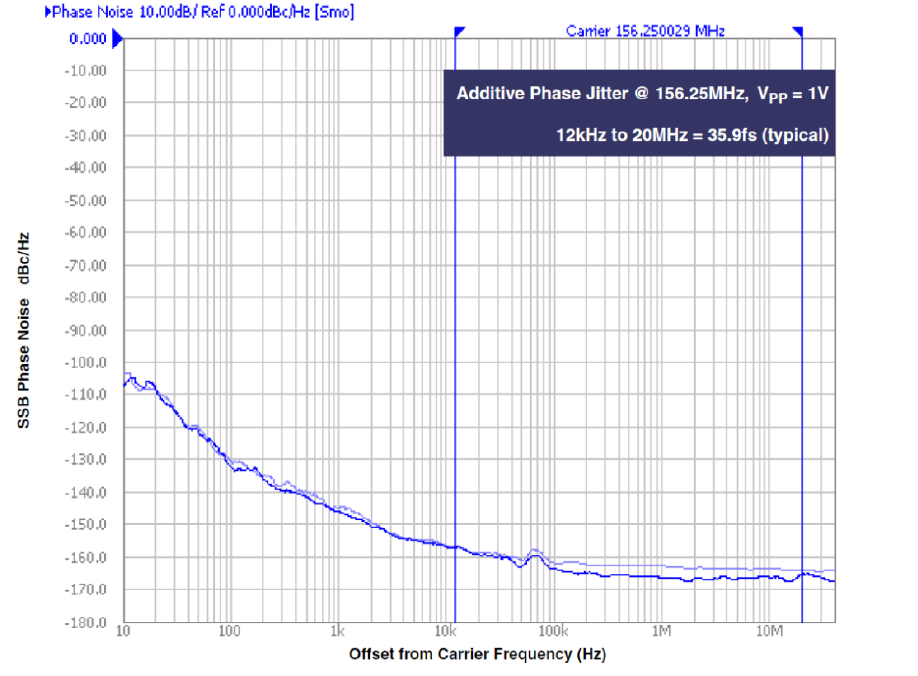
To get the correct number, one needs to square the RMS Phase Jitter of the output (light blue PN curve), subtract the square of the RMS Phase Jitter of the input (dark blue PN curve), and then take the square root of the result; effectively performing the Square Root of the Difference of the Squares. Note that this value is still dependent on both the frequency and the integration range of interest. So, both must be qualified when specifying the “additive” RMS Phase Jitter of a Fan-Out Buffer. This same Figure 9 is actually the PN Plot from the device datasheet of the IDT 8SLVP1208 Low Phase Noise 1:8 LVPECL Fan-Out Buffer. For this device, the “additive” RMS Phase Jitter for a carrier frequency of 156.25MHz, integrated from 12KHz-to-20MHz, is ~ 35.9fs.
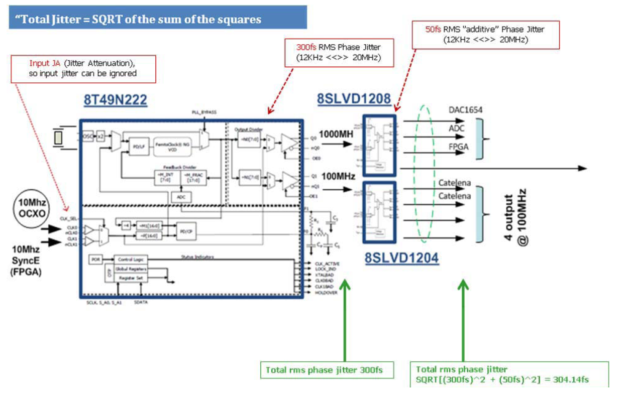
Quantifying the “additive” RMS Phase Jitter in this manner allows the total RMS Phase Jitter to then be correctly calculated as the Square Root of the Sum of the Squares. Consider the 1GHz ADC/DAC Clock Distribution example shown in Figure 10. In this example, the first stage PLL has 300fs of intrinsic jitter generation. And, the subsequent FOB driven by this PLL has an “additive” RMS Phase Jitter specification of 50fs. The resultant total RMS Phase Jitter of the 1GHz clock provided to the ADC is calculated as follows:
total RMS Phase Jitter = SQRT[(300fs)2 + (50fs)2] = 304.14fs.
It is worth noting that the “additive” effect of the FOB used in this example is still very low, adding only ~4fs to the total RMS Phase Jitter.
Conclusion
Frequency domain jitter is typically measured as Phase Noise and is a measure of the instantaneous phase deviations from the ideal; effectively a frequency domain quantification of clock jitter. Typically, this type of jitter is expressed as a PN Plot that shows the dBc values at the various carrier frequency offset points. It can also be quantified as RMS Phase Jitter, qualified with the application appropriate integration band of interest. This type of jitter is relevant for High Speed Serial communication and ADC use cases, to name just two. In addition, spurious content from a PN Plot should also be quantified in order to characterize the total clock jitter.
Integrated Device Technology, Inc.
www.idt.com

Leave a Reply
You must be logged in to post a comment.