Engineers who design power circuits around wide-bandgap semiconductors frequently make costly mistakes that relate to the switching behavior of transistors.
Julian Styles | GaN Systems
We need to face an awkward and embarrassing truth about ourselves in the world of power electronics. I’d like to ask you to try to be completely open and honest for a moment.
Are you mistaken about the body diode?
Many engineers are. We all have similar origin stories about how this confusion started.
MOSFETs have an extremely useful property; that is, when VGS=0, they still conduct in reverse. They do this because they have a parasitic diode between source and drain called an intrinsic body diode. When learning power electronics, we all discovered that MOSFETs can conduct in reverse (because they have a body diode) and IGBTs can’t (because they don’t).
Because “reverse current path with gate off” is kind of a mouthful, we all got accustomed to just referring to this effect as a “body diode.” And everything was fine, for decades. Then new wide-bandgap devices came along. Because of their construction, some don’t have parasitic diodes. But they still have the same useful property as MOSFETs: They conduct in reverse when VGS=0. Most notably, GaN E-HEMTs have this property.
And so the confusion began.
My colleagues and I have had many, many meetings with engineers who assume that, because GaN devices do not have body diodes, they do not conduct in reverse. We’ve had countless conversations similar to this one:
Engineer: “So GaN Devices don’t have a body diode?”
Me: “Correct.”
Engineer: “So they can’t conduct in reverse with VGS off? So I need to add an anti-parallel diode?”
Me: “Incorrect.”
Cue engineer’s head exploding.
It is time we update our terminology so we can accurately refer to the reverse conduction path, understand why body diodes are not necessary for this feature, and even appreciate the benefits that GaN devices bring to the world by having no body diode.
What’s actually going on
In GaN E-HEMTs, a lateral two-dimensional electron gas (2DEG) channel formed on an AlGaN/GaN hetero-epitaxy structure provides extremely high charge density and mobility. For enhancement-mode operation, a gate intrinsically depletes the 2DEG underneath the gate electrode at 0 V, or negative bias. A positive gate bias draws electrons into the depleted area and turns on the 2DEG channel. In forward conduction (first quadrant), this behavior works much like that of a MOSFET but with better switching performance.
In the third quadrant, (VGS =0, VDS negative), the device behaves differently than a MOSFET. In simple terms, the negative bias on the drain terminal creates a voltage gradient in the device channel. This, in turn, causes the depletion region under the gate to have a negative electrical potential relative to the gate electrode. In other words, the drain of GaN HEMT will behave as the source and the source will act as the drain. Once the potential difference between the gate and the channel exceeds the threshold voltage (VTH_GD) of the device, the device turns on, an effect sometimes called “self-commutation.” Because the device is conducting current, I, through its (resistive) channel, Ron, the voltage drop D is
D = VTH_GD + IRon
If the device is turned off with a negative voltage, the drain must be more negative before self-commutation arises, and the total voltage drop DT is
DT = VTH_GD + (-VGS) + IRon

A diagram from the GaN Systems’ application note GN001 shows IR curves for different values of VGS.
Confession time. GaN device manufacturers have had a role in perpetuating our misunderstanding of the reverse conduction path.
Over the years, GaN manufacturers have taken two main approaches to explain how their devices behave when reverse biased with VGS=0. First, some manufacturers simply kept using the term “body diode.” They explained that GaN devices have a magical body diode with zero QRR (reverse recovery charge) and a surprisingly high voltage drop. This is not true, but rather a convenient fiction that allows designers to design successful circuits most of the time.
Second, some manufacturers publish detailed documentation of their device’s behavior with the expectation that engineers would carefully read the manual, realize the potential for error, and change their ways before considering the technology – a commendably honest approach, yet perhaps overlooking that engineers are human beings, and ingrained habits are difficult to change.
As you might expect, the outcome of these approaches is confusion. To this day, GaN Systems’ field application engineers see customer design schematics that show our devices with added anti-parallel diodes to provide a freewheeling current path.
Benefits of no body diode
It’s a shame that this misunderstanding of GaN devices’ lack of a body diode persists. After all, there are some real benefits to reverse conduction without a body diode.
First, no body diode means no QRR, making GaN suitable for half-bridge hard switching. This, in turn, means no additional hard commutation due to the diode reverse recovery, which otherwise leads to much higher switching losses. The zero reverse-recovery of GaN also enables new high-efficiency topologies such as bridgeless totem pole PFC (power factor control).
Second, the absence of a body diode means no burst of diode noise when the body diode turns on. This makes EMI design simpler and boosts performance. It is especially helpful in compact designs where power conversion and signal processing are on the same small PCB.
Finally, there are benefits in dv/dt limits and reliability. MOSFETs have a failure mechanism caused by high dv/dt on the MOSFET body diode. While the body diode is in reverse recovery, its drain-source voltage rises. This behavior can cause a false turn-on of the internal parasitic NPN bipolar transistor, destroying the MOSFET.
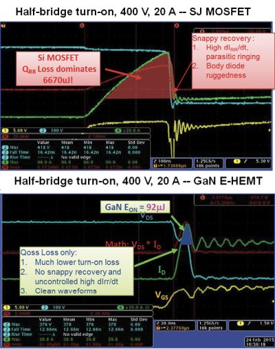
Switching waveforms of a typical MOSFET and E-HEMT illustrate some of the differences in turn-on behavior caused by the body diode.
There is really only one disadvantage of having no body diode: higher reverse voltage drop. The reverse voltage drop of a GaN E-HEMT includes a resistive element arising from the channel resistance and threshold voltage. The voltage drop in a 650-V GaN E-HEMT can be as much as 3 V when conducting large currents, larger than the equivalent drop in a MOSFET. This higher reverse voltage drop has the potential to reduce efficiency by increasing losses in the dead time of a typical half-bridge circuit.
Fortunately, these losses can be reduced by shortening the dead time. The fast switching behavior of GaN E-HEMTs usually simplifies the task of shortening the dead time. In addition, embedded packages for GaN devices, such as GaN Systems GaNPx package, have low parasitic inductance, which ensures reliable switching transitions with shortened dead time.
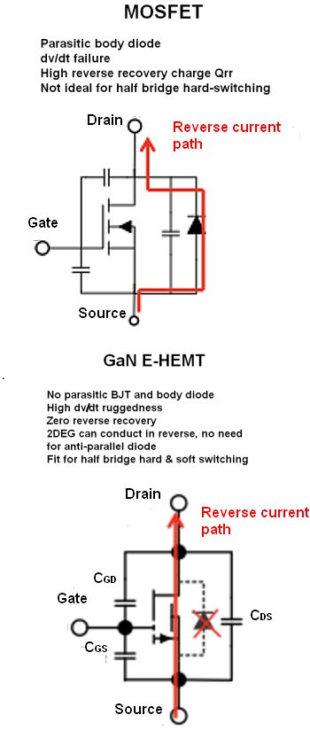
The differences between reverse conduction in MOSFETs and GaN HEMTs.
Generally, GaN circuit implementations see an efficiency gain from shortening dead time that significantly outweighs the losses from higher reverse voltage drop. It is easier to realize this efficiency gain as new-generation drivers and controllers increasingly support shorter dead times.
It’s also worth noting that a short dead time is good for other reasons. For example, in Class D audio amplifiers, a shorter dead time leads to lower harmonic distortion and higher audio quality.
There is a lot of help available for those who want to shake off the stigma of body-diode-wrongness and create designs optimized for efficiency and low cost. We can always create T-shirts with slogans like, “I ain’t got no body (diode)” and “Ask me about reverse conduction.” Joking aside, a better understanding about the facts regarding the body diode and a clear explanation of how GaN devices operate help clear up confusion, at least until the next evolution of power devices trigger a new set of definitions.
REFERENCES
Design/High side driver considerations
Recommended GaN driver/controller ICs


Leave a Reply
You must be logged in to post a comment.