LiDAR systems and ToF techniques are critical to providing self-driving cars with a detailed picture of the surrounding and is used in many research applications as well. This is part three of a four-part series on LiDAR systems and ToF techniques.
At the front end of a LiDAR system is the photon emitter and its corresponding receiver. This part looks at these components and issues of pulse rate, power, pulse width, and more. The choice of wavelength to use is a tradeoff, as the wavelengths at which the emitters excel are not the same as those of the sensor, plus there are issues of atmospheric absorption and the solar-radiation spectrum (Figure 1).
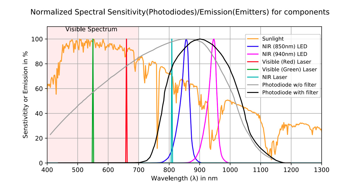
Fig 1: Spectral response of different emitters and photodiodes in comparison with solar spectrum. (Image: Texas Instruments)
The photon emitter
The front-end of a LiDAR system begins with the photons emitted by an electronically controllable source. In the earlier LiDAR days, the only source which had the needed characteristics was a pulsed laser diode (PLD), typically operating at 950 nm due to low atmospheric absorption. Other wavelengths were used in some installations due to issues of efficiency and other factors. Peak power of the APDs is about 50 to 100 W.
In recent years, there has been a trend to using infrared LEDs (IR LEDs) as their power output has increased to a suitable level, and their easier drive and control. Further, the IR LED as emitter is eye-safe under all conditions, with no need for Laser Class 1 safety precautions and associated regulatory concerns. LEDs also require less electrical power compared to PLDs, and the difference of a few watts is not make-or-break in the totality of an automotive LiDAR system which requires hundreds of watts and more. However, it does mean that less current has to be delivered the emitter assembly resulting in lower DC voltage drop (called IR drop, but “IR” here does not mean infrared, it means current × resistance) and the thermal dissipation is also reduced.
The photon sensor
As the reflected photons return to the LiDAR system, they must be captured and converted into an electrical signal and current. The two sensor types most often used are the conventional PIN photodiode (positive-intrinsic-negative) and the silicon avalanche photodiode (APD).
PIN diodes use the photoelectric effect to create hole-electron pairs called charge carriers which then deliver a photocurrent. (This effect is an easily observed physics and optical phenomenon which posed a major theoretical conundrum, and which was resolved by Albert Einstein; he received the Nobel Prize for his radical explanation, not for relativity). While the PIN diode works, the conversion ratio of photons to electrons (the transfer ratio) is modest, so the sensitivity is low and more received photons are needed for measurable current. Also, internal diode and circuit noise can obscure the generated electrons, adding to SNR weakness.
APDs expand the photoelectric principle by accelerating the charge carriers in an electric field (and so need a higher-voltage source). The use of the electric field results in additional electron-hole pairs through what is called impact ionization. This is similar to the vacuum-tube photomultiplier tube (PMT), but is smaller and with a not-as-high voltage; however, there is more noise and a lower transfer ratio compared to the PMT.
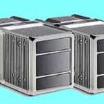
As a consequence of the APD operation, a single photon may produce hundreds or even thousands of electrons from a single photon and this higher current. A single APD may not deliver sufficient resolution and conversion gain. For this reason, APDs are often used in arrays of 8, 12, 16, or even 64 elements (Figure 2). Resolution is also determined by the pixel pitch (spacing between the APDs) which can be as tight as 40 µm.
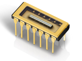
This array combining low-noise, high-sensitivity silicon avalanche photodiodes in a monolithic assembly; the arrays have been optimized for the 800-900 nm wavelength range and include a low temperature coefficient and a gap of only 40 µm between elements. (Image: Laser Components)
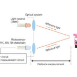
The signal-conditioning electronics of the APD interface are obviously critical as well. The optimum internal gain of the transimpedance amplifier which interface with the APD is selected to match the internal noise of the APD with the input noise of the amplifier and its load resistance, so the APD does not increase system electronic noise (Figure 3). The tradeoff is that noise increases with the bandwidth of the system for both APDs and PIN diodes, so it is desirable to reduce bandwidth as much as can be tolerated without degrading system throughput.
PIN diodes and APDs are available from many vendors, including Hamamatsu, First Sensor, Osram Opto Semiconductors, and Laser Components, and a full list is much, much longer. These are highly specialized components and their suppliers range from small “boutique” sources to much larger but still niche suppliers who focus almost exclusively on electro-optical sources and sensors and little else. This is not surprising as the world of photonics components requires very different materials, expertise, processes, and tests compared to “conventional” electronic devices based on silicon, SiC, GaAs, or other elements and compounds.
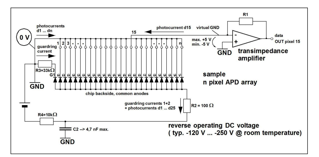
Fig 3: The interface transimpedance amplifier for the PIN diode or APD must be matched to the characteristics of the specific sensor for lowest-noise and highest-sensitivity performance. (Image source: First Sensor AG)
Scanning the LiDAR
A single pulse will just tell you what is out there in one direction (a vector) but not create an image. To do this, the electronics of many LiDAR systems use a highly refined version of an “ancient” optical fixture: a spinning-mirror scanning galvanometer (Figure 4).
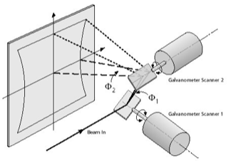
This is the cylindrically shaped object seen on top of many autonomous cars. The mirror assembly rotates at between one and ten revolutions per second as well as up and down. It directs the pulsed light around the 360⁰ circle and also directs the reflected bean back to the photosensor. Some mirror assemblies do not rotate around the full circle; instead, they scan back and forth over a limited angle for faster scanning.
As with any technology, there are many variations in how the actual design is implemented. Rotating LiDARs are fairly bulky and mechanical, needing special mounting to work in the harsh automotive environment. One type of solid-state LiDAR uses micro-electromechanical system (MEMS) technology with a MEMS-based based mirror moves to “scan” the environment, often based on Texas Instruments digital light projector (DLP) MEMS components. Another technique used in solid-state LIDAR is an optical phased array (OPA) with multiple independent sources that dynamically direct and target the pulses in different direction by adjusting the array timing and does not require sensor movement. OPA-based LiDAR is more durable and reliable as it does not move and it also enables fast scanning, smaller size, but price is an issue.
Unlike scanning LiDAR, flash LiDAR does not move the light or laser at all. Instead, it works like a camera, delivering a flash of light to detect the whole surrounding area at once and analyzing the information with image sensor. The light source of flash LiDAR is more powerful, but the detecting distance and field of view are much lower than with scanning LiDARs. As the pulse rate has increased while the pulse width has decreased, there are the usual issues of high-speed driver circuitry, parasitic inductance, drive-waveform fidelity, and the need to keep the driver compact and close to its load, the optical emitter.
At present, there is no non-moving, solid-state scanner which can provide 360 degrees of coverage; instead, multiple arrays with some overlap must be used. There’s some irony that the relatively “ancient” mechanical assembly is still the widely used approach, working in conjunction with advanced components and electronics such as laser diodes and high-performance graphics computing engines. Reality is that as a mature (but still evolving) device, a well-designed mechanical unit can be relatively reliable and compact, as a result of decades of experience with their implementation and likely weak points. Still, a design without moving parts is very attractive, and there are some units available.
The final part of this article looks at some hardware issues and available implementations.
EE World References
- Autonomous vehicle sees with LiDAR eyes
- A better way to measure lidar
- How can picture-like images be obtained from LiDAR?
- Doppler Lidar for Autonomous Cars Excels in Real-World Tests
- At Autonomous Vehicle Sensors Conference: Upstart Lidar Companies Face Off
- GaN FET driver excels at solid-state light detection and LiDAR apps
- What advanced sensing techniques are used to find lost treasures? Part 5: LiDAR
- The Future Of LIDAR For Automotive Applications
- LiDAR: How The Next Generation Of Radar Mapping Works
- Vacuum tubes we still (have to) use: The photomultiplier tube, Part 1
- Vacuum tubes we still (have to) use: The photomultiplier tube, Part 2
External References
- IEEE Spectrum, “Lidar-on-a-Chip: Scan Quickly, Scan Cheap”
- Tech Briefs, “Real-Time LiDAR Signal Processing FPGA Modules”
- NASA, “A Survey of LIDAR Technology and its Use in Spacecraft Relative Navigation”
- Laser Focus World, “Lidar advances drive success of autonomous vehicles“
- DARPA, “SWEEPER Demonstrates Wide-Angle Optical Phased Array Technology”
- NOAA, “What is LIDAR?”
- Terabee, “Time of Flight principle”
- Terabee, “A Brief Introduction to Time-of-Flight Sensing: Part 1 – The Basics”
- AMS AG, “Time-of-Flight Sensing”
- All About Circuits, “How Do Time of Flight Sensors (ToF) Work? A Look at ToF 3D Cameras”
- Texas Instruments, “ToF-based long-range proximity and distance sensor analog front end (AFE)”
- Texas Instruments, “Time of flight (ToF) sensors”
- Texas Instruments, SBAU305B, “Introduction to Time-of-Flight Long Range Proximity and Distance Sensor System Design”
- Texas Instruments, OPT3101 Data Sheet
- National Center for Biotechnology Information, S. National Library of Medicine, ”A Fast Calibration Method for Photonic Mixer Device Solid-State Array Lidars”
- Yu Huang, “LiDAR for Autonomous Vehicles”
- Geospatial World, “What is LiDAR technology and how does it work?”
- American Geosciences Institute, “What is Lidar and what is it used for?”
- National Ecological Observatory Network (NEON), “The Basics of LiDAR – Light Detection and Ranging – Remote Sensing”
- Hamamatsu Photonics, “Photodetectors for LIDAR”