by Claudia Relyea, Revanth Reddy Pappireddy, and Sandeep Koranne, Mentor Graphics
Metal-insulator-metal and metal-oxide-metal capacitors popular in analog/RF designs because of their desirable characteristics. By extracting parasitics from your models that are important in your design, you’ll get a robust circuit.
Analog and RF IC designs are essential to many of the communications technologies now in use and in development, including 5G cellular technology, mobile applications, and the Internet of Things (IoT), a network of smart devices connected to the internet to share data. End users across different industries and services, from business to education to entertainment to transportation, are looking for improved integration, more efficient power management, and high RF/ extremely high frequency (mmWave) [1] performance.
Process technologies using fin field-effect transistors (FinFETs) and fully-depleted silicon-on-insulator (FDSOI) transistors allow designers to integrate a wide spectrum of high-performing RF and mmWave transistors with logic devices to address a variety of market segments, including mobile, IoT, analog, and RF/mmWave [1,2].
While 5G will deliver unprecedented bandwidth and multi-gigabit data rates, it also faces power management challenges and high-power linearity requirements [3]. Capacitors are an integral part of many analog/RF design applications, with metal-insulator-metal (MIM) and metal-oxide-metal (MOM) capacitors being widely employed. Unfortunately, process variations and in-context issues can affect capacitive accuracy and matching requirements, making accurate extraction and modeling both essential and more complex. In this article, we’ll focus on the design and parasitic extraction (PEX) challenges of MIM/MOM capacitors in RF design applications, and propose best practices to solve those challenges, illustrated by experimental results.
Capacitors
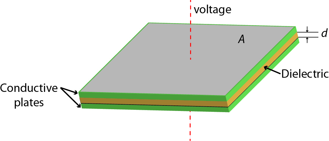
The simplest type of capacitor consists of two overlapping parallel plates separated by a dielectric (Figure 1). The plates act as electrical conductors and the dielectric as an insulator. When a voltage difference is applied across the conductors, an electric field is created across the dielectric, which causes a positive charge to collect on one plate and a negative charge on the other plate. The capacitance (C) between the plates is a function of the area of the overlapping plates (A), the dielectric constant (ε), and the distance (d) between the plates (C=εA/d)it is also the ratio of the electric charge (Q) on each conductor to the voltage difference (V) between them (C=Q/V).
 Capacitors in analog/RF design
Simple plate capacitors require a lot of area, though, and can’t be tuned. In a bandpass filter (also known as LC tuning circuits), charge flows between the capacitor plates and through an inductor connected to the plates to store electrical energy in specific resonant frequency bands. Bandpass filters are key components in oscillator, filter, tuner, and frequency mixer designs [4], and are commonly used in analog/RF designs when a tunable frequency source is needed, such as in signal generators, radio transmitters, and receivers.
Capacitor design requirements for analog/RF circuits include low voltage coefficients, good capacitor matching, precision control of capacitor values, and small parasitic capacitance. In addition, designers strive for high reliability and low defect densities in manufacturing [5]. Because of these requirements, on-chip capacitors in a bank must match very precisely, and deliver capacitance density, voltage linearity, leakage current, and a quality factor (Q-factor) that comply with the design specifications. In the past, designers were forced to compromise between the Q-factor and capacitance density. Advanced process technologies now enable smaller feature sizes and an increased number of metal layers. With these technologies, capacitors can be created using multiple vertical metal layers on existing masks, which maximizes both capacitance density and Q-factor, and provides inherent symmetry [6].
Capacitive charge pumps use capacitors to raise or lower voltage; they’re integral components of an analog to digital converter (ADC). In an ADC charge pump, voltage gain is achieved by sampling an input voltage on multiple capacitors, and subsequently connecting each capacitor in series to yield a total voltage equal to the sum of the individual voltages sampled on each capacitor [7]. Due to this relationship, charge pumps require precise capacitance matching, because even a small error on each capacitance changes the output voltage significantly [8].
MIM/MOM capacitors
Metal-insulator-metal (MIM) and metal-oxide-metal (MOM) capacitors are widely used in analog/RF designs because of their desirable characteristics:
- High-capacity density due to minimum width and spacing of metals
- Good matching characteristics due to lateral coupling
- Symmetric plate design
- Superior frequency characteristics and quality factor
- Low cost, due to no additional mask or process steps [9]
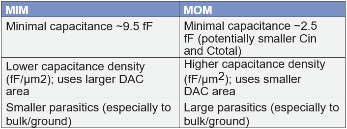
Each type, however, has specific pros and cons, so designers must weigh those factors to decide which device is best suited for a particular application. Table 1 provides a list of design considerations for a capacitive digital-to-analog converter (DAC), part of a 10-bit successive-approximation-register (SAR) ADC design.
A MIM capacitor consists of parallel plates formed by two metal planes separated by a thin dielectric [11]. MIM capacitors are used in RF circuits for oscillators, phase-shift networks, coupling, and bypass capacitance. They are also useful for analog design, due to their highly linear nature and dynamic range [5]. Special processes exist to create MIM capacitors, and these devices are usually formed in additional top layers of the stack. For example, in the IBM CMOS10LP/RFe process technology, a MIM capacitor is formed by adding two masks between the last metal and terminal aluminum layers. [12].
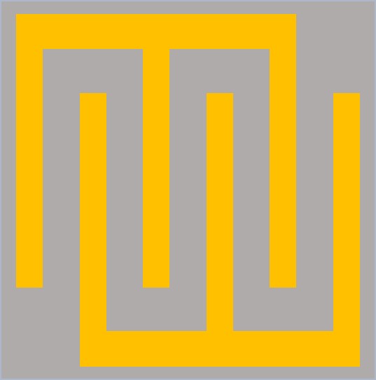
A MOM capacitor is constructed of multiple inter-digitated fingers (Figure 2). It can be formed with metal interconnect layers and doesn’t require additional masks. When using multiple metal layers in the construction, the capacitance density for the capacitor can be increased, exceeding that of a MIM capacitor [13].
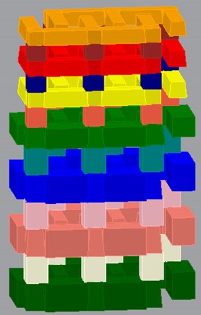
A vertical natural capacitor (VNCAP), also known as a vertical parallel plate (VPP), is a type of MOM capacitor made up of inter-digitated fingers on multiple stacked metal layers (Figure 3). The fingers are connected by vias. This type of construction increases the capacitance per unit area. Modeling shows that a square VNCAP device often provides the best trade-off between high capacitance values and high Q-factor [12].
A vertical natural capacitor (VNCAP), also known as a vertical parallel plate (VPP), is a type of MOM capacitor made up of inter-digitated fingers on multiple stacked metal layers (Figure 3). The fingers are connected by vias. This type of construction increases the capacitance per unit area. Modeling shows that a square VNCAP device often provides the best trade-off between high capacitance values and high Q-factor [12].
Experimental results further show that VNCAPs have excellent capacitance density, Q-factor, symmetry, and vertical scalability, and are compatible with existing CMOS technologies, making them suitable for RF applications [6].
Process variations can, however, affect capacitive accuracy and matching requirements, making accurate capacitor modeling both essential and more complex. One important part of that modeling is accurate and precise PEX. Let’s take a look at how designers are achieving design and verification goals with the use of innovative PEX technology.
MIM/MOM parasitic extraction best practices
PEX is a required stage in the design flow. PEX tools enable designers to model parasitic effects on their circuit design in functional simulations and perform post-layout analyses. With these, you can determine if the manufactured chip will still perform according to design specifications. The stringent design accuracy requirements for MIM/MOM capacitor designs translate to precise extraction requirements for a PEX tool. Effects modeled during capacitor PEX flows include electrical characteristics, such as:
- Coupling capacitance between plates
- Coupling cap between plates to substrate
- Coupling cap between plates and surrounding nets
- Capacitance matching
In addition, modeled effect include frequency characteristics to calculate quality factor and resonant frequency [9]. Parameters include impedance and equivalent series resistance.
Foundries provide pre-characterized parasitic models for certain cells and devices in a specific process technology. Depending on the sensitivity and criticality of these cells/technologies, the models may cover a few specific or all parasitic effects [14]. Due to the high degree of accuracy required in parameter extraction during the generation of an accurate SPICE model for these devices, foundry device characterization is typically done using a full-wave, frequency domain electromagnetic solver that can also calculate scattering, admittance, and impedance (S,Y,Z) parameters and resonant frequency. Such solvers are highly accurate, but extremely slow, which is an acceptable tradeoff for the device characterization process but isn’t practical in design verification flows.
Some foundries also use silicon measurements for their device models, which allows them to include effects (such as retargeting) that are not normally handled by table-based RC extraction tools. Local effects such as bias, width, and spacing can also be included. However, some layout context-specific effects cannot realistically be captured in a model, so foundry models may assume overly pessimistic conditions to account for capacitive interaction between the content of the cell and the design context.
At advanced nodes, these non-local effects, such as density, loading, thickness, and double patterning (DP) coloring mask shifts, play a very large role in capacitance accuracy. In other words, because the parasitic coupling effects of the routing adjacent to, above and below the device affect the device characteristics, the PEX process must be context-aware—that is, it must be able to recognize and take these effects into account—to ensure the highest accuracy in the results. Context-aware PEX is especially important for DP mask layers.
For example, since MIM capacitors are manufactured in the upper metal layers, there is usually routing on the lower metal layers beneath these devices that changes the coupling capacitances in the device region. Because this routing differs from design to design, foundries typically don’t supply pre-characterized models for MIM capacitors; instead, they expect designers to use context-aware PEX tools to model these devices. Conversely, due to the location of MOM capacitors in the metal stack, these context effects don’t exist, so designers have the option to use a pre-characterized model provided by the foundry.
RF designers’ need for very accurate device extraction—including the extraction of parasitics inside of the device region, as well as the parasitic interaction of the device geometries with the in-context routing—represents a new application for PEX tools. Flat extraction of designs down to the device level, including device geometries, requires faster performance and higher capacity than a full wave field solver (which takes into account all terms of Maxwell’s equations) can provide, but higher accuracy than conventional rule based PEX tools are designed for.
Parasitic effects inside the device region
MOM and MIM capacitors contain a combination of large and small geometries. To provide faster performance, traditional pattern-matching-based PEX tools use analytical formulas to make approximations of parasitic effects, and are not designed to compute fringe capacitance effects in the presence of dielectrics. Since MOM capacitors have a significant amount of fringe and coupling capacitance between the metal comb structures (Figure 4), even close approximations can have a significant negative impact on accuracy.
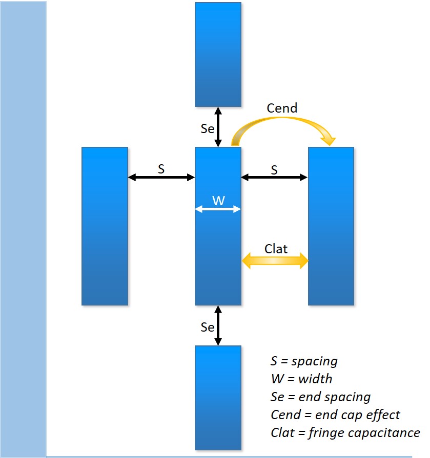
Other important parasitic effects that must be modeled are line-end capacitance and line-end fringe capacitance. These effects are particularly significant in single-layer MOM capacitors because the wires are short enough that end (Cend) or fringe (Clat) effects can contribute around 10% to the total capacitance, meaning a simple capacitance per unit length calculation is insufficient (Figure 5).
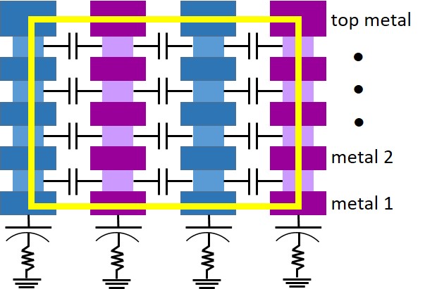
In the VNCAP device shown in Figure 6, the coupling capacitances between the interdigitated fingers (inside the yellow outline) are amplified by the multiple stacked metal layers.
For example, a designer may opt not to use foundry-supplied alternate polarity MOM (APMOM) devices because they were designed with psub guard rings, which require too much area. In another case, foundry-supplied capacitor devices may use poly and diffusion layers to improve substrate shielding, but designers may prefer to use nwell or deep nwell to minimize substrate coupling capacitance. For these types of applications, designers must extract both the substrate coupling capacitance and the coupling capacitance between the plates and to neighboring nets, and ensure excellent capacitance matching between the neighboring cells when the devices are placed in the context of their designs.
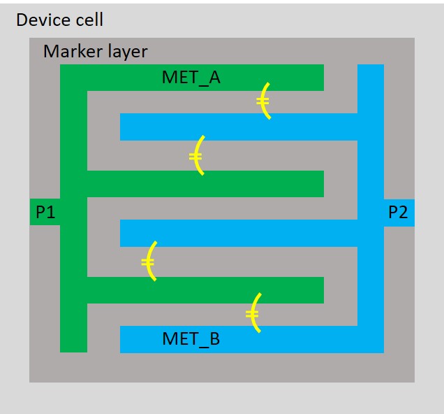
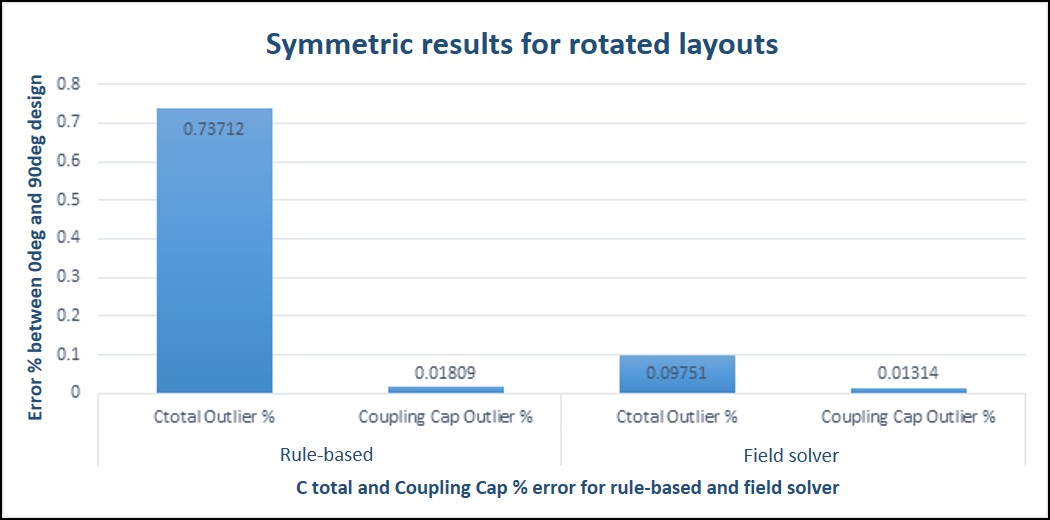
Another concern for analog designers who must achieve matching for filters is symmetry. When MIM/MOM capacitors are placed in the design context, the instantiations can be reflected or rotated in different directions. A field solver is inherently able to produce consistent accurate results for all of these symmetric instances. A rule-based engine’s capacitance results typically show small variances, due to scan line direction or binning differences. To ensure accuracy, these extraction engines must be designed to eliminate the effects of any such differences (Figure 7).
PEX at the block level
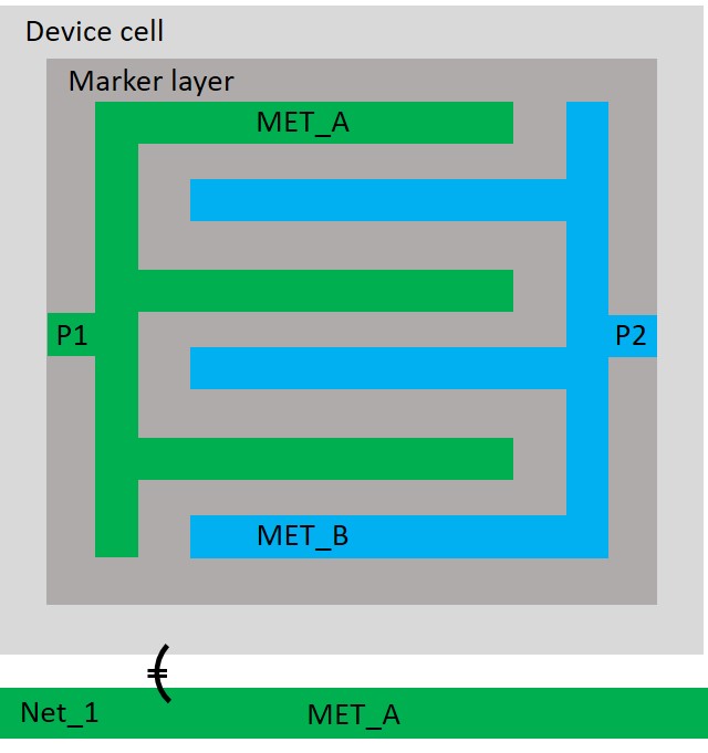
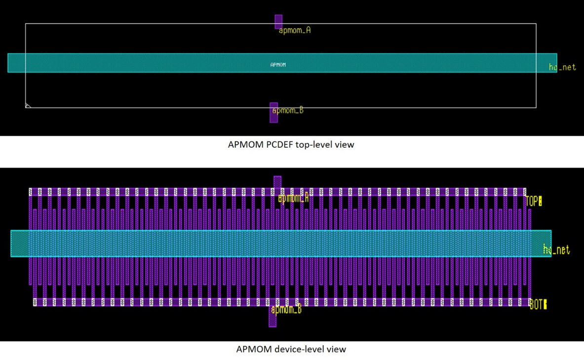
Accurate capacitor matching is also important for block-level extraction. In addition, the coupling capacitances from designed capacitors to the surrounding signal nets must be reduced as much as possible, and must match very closely. Devices such as MOM capacitors can be instantiated as pre-characterized cells (pcells) in the layout, and PEX can be run on this configuration (Figure 8). This pcell device (PCDEF) cell-based RC blocking (xcell) flow helps to speed up extraction at the block level, because only the parasitics between cells and between cells and adjacent signals are extracted.
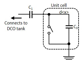
An example of a suitable application of the PCDEF xcell extraction flow is in DCO design. A DCO contains several capacitor banks, some of which are used to modulate the RF carrier during a transmission. Each capacitor bank contains multiple unit capacitors that can be switched on or off (Figure 9).
In each case, the unit capacitor cell has a certain capacitance value. The designer is interested in the difference in capacitance between the on and off states. Equally important, when turning on one or more unit cells inside the capacitor bank, each activated unit cell should have the same increase in capacitance. Each unit cell is preceded by a capacitor (C1) that connects the unit cell to the DCO tank. The delta capacitance is the difference in capacitance presented to the DCO tank when the switch is open or closed and can be influenced by unwanted coupling between the unit cells and other circuitry inside the capacitor bank.
The unit cells are arranged in a binary way. This means that activating bit 0 increases the capacitance, with a value equal to activating a single unit cell (=LSB). Activating bit 1 increases the capacitance by 2x the unit cell capacitance, while activating bit 2 increases the capacitance by 4x. The delta capacitance between each binary step should be consistent. To ensure this delta capacitance remains consistent, the number of unit cells placed in parallel is changed; for bit 0 (B0), there are eight unit cells in parallel, for bit 1 (B1), four unit cells in parallel, and for bit 2 (B2), two unit cells in parallel.
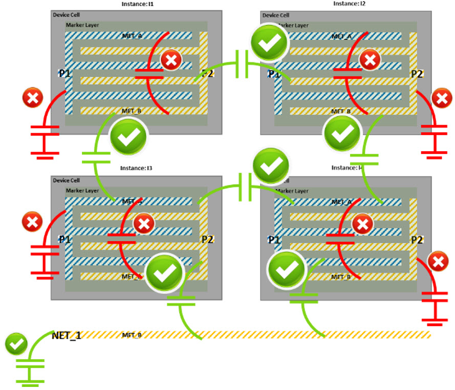
During extraction of this design, the MOM capacitors are marked as pcells and their contents are not extracted. Only the interactions between the routing and the pcells are modeled. For nets that exit a pcell through a pin, the coupling capacitance between neighboring nets and nets inside the pcell is extracted. These parasitic capacitances are marked in green in Figure 10. For nets internal to the pcell, the coupling capacitance is computed to the neighboring nets outside the pcell, lumped to ground, and accounted for on the neighboring net. These parasitic capacitances are marked in red in Figure 10. The intentional device in the pcell can also be netlisted.
The advantage of this PCDEF xcell extraction flow is that the designer can choose to extract only the parasitics that are critical in the context of the design. This flow avoids double counting of parasitic effects inside the pcell that are already accounted for in the SPICE model supplied by the foundry. The resulting netlist containing the parasitic RC elements together with the intentional devices can then be instantiated in a post-layout simulation testbench, and used to evaluate the effects of interconnect parasitics on the performance of the design.
Extraction results
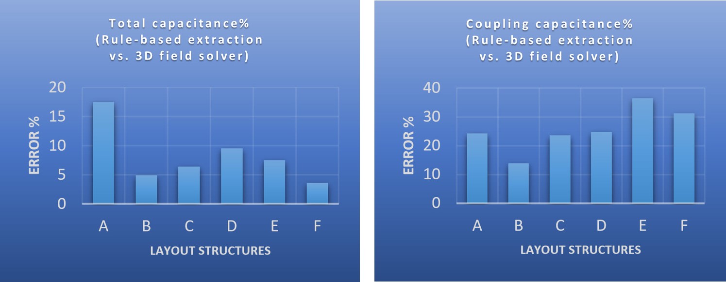
To develop and test these best practices, we used the Calibre xACT platform, with integrated Calibre xACT 3D field solver and Calibre xL inductance extraction functionality. Unit device tests were run to compare the accuracy of a rule-based extraction tool to a 3D field solver for multiple device structures, as shown in Figure 11. For most of these structures, the total capacitance of the device as extracted with the Calibre xACT tool is within 10-15% of the Calibre xACT 3D field solver results. For device A, the total capacitance error is higher (15%), because line-end effects dominate the parasitic capacitance. The coupling capacitance, on the other hand, can vary as much as 30% to 40%, due to the geometric properties of the capacitor devices. If designers are concerned about modeling these types of effects with higher accuracy, they can opt to use the Calibre xACT 3D field solver for PEX, which supplies the required accuracy with much faster performance than a full-wave field solver, and has the capacity to extract even large blocks.
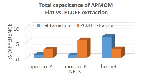
Experiments were also done using a MOM capacitor device (Figure 12) to compare the extraction accuracy of designs using pcells vs. flat device-level extraction.
Results show that the accuracy of pcell extraction match up very closely to flat extraction results, meaning a pcell extraction flow can be used for analog/RF designs using devices containing foundry-supplied pcells (Figure 13). Both the Calibre xACT and Calibre xACT 3D tools support this type of extraction mode, allowing the designers to select the extractor type based on their accuracy requirements.
Summary
The extensive use of capacitors, particularly MIM/MOM capacitors, in analog/RF designs presents a variety of PEX challenges to designers. These designs typically require a combination of both rule-based and field-solver-based extraction, as well as context aware functionality, to ensure designers can obtain accurate results in a timely manner. Understanding best practices for extracting the complex geometries of capacitor devices, as well as the in-context coupling effects for those devices in sensitive analog/RF blocks, enables designers to accurately apply the appropriate extraction process to different parts of the design.
References
- Wikipedia contributors, “Extremely high frequency,” Wikipedia, the Free Encyclopedia, https://en.wikipedia.org/wiki/Extremely_high_frequency (accessed February 24, 2020).
- TSMC, “16/12 Technology,” https://www.tsmc.com/english/dedicatedFoundry/technology/16nm.htm
- Thomas, “Evolving 5G Landscape Creates New RF Challenges,” Electronic Design. July 24, 20218. https://www.electronicdesign.com/power/evolving-5g-landscape-creates-new-rf-challenges
- Wikipedia contributors, “LC circuit,” Wikipedia, The Free Encyclopedia, https://en.wikipedia.org/LC_circuit (accessed January 3, 2020).
- S. Chang, “Applications of Metal-Insulator-Metal (MIM) Capacitors,” International SEMATECH, August, 2000. https://pdfs.semanticscholar.org/f89e/16bff9396031f251441eb73b8f708bb3699d.pdf
- Kim, et al. “Symmetric Vertical Parallel Plate Capacitors for On-Chip RF Circuits in 65-nm SOI Technology,” IEEE Electron Device Letters, vol. 28, no. 7, pp. 616-618. July 2007. https://cycho.org/public/paper/DKim_EDL2007_VPPCap.pdf
- Ahmed, J. Mulder, D. Johns, “A Low-Power Capacitive Charge Pump Based Pipelined ADC,” IEEE Journal of Solid-State Circuits, vol. 45, No. 5, May 2010. https://iadc.ca/pdf/Ahmed_Johns_Mulder_JSSC_May2010.pdf
- Pylarinos, “Charge Pumps: An Overview,” IEEE International Symposium on Circuits and Systems, 2003. https://pdfs.semanticscholar.org/dc21/19b41d71abdadeac5de771daf80a404d7134.pdf
- Ershov, “MOM capacitor simulation challenges and solutions,” Silicon Frontline Technology. https:// designers-guide.org/forum/Attachments/MOM_capacitor_design_challenges_and_solutions_SFT_200904.pdf
- Moron, et al., “Development of ultra-low power 10-bit SAR ADC in 65 nm CMOS technology,” Topical Workshop on Electronics for Particle Physics (TWEPP), Sept. 2019. https://indico.cern.ch/event/799025/ contributions/3486155/attachments/1902197/3140411/moron_TWEPP_ADC_2019_09.pdf
- Niknejad, “Lecture 7: IC Resistors and Capacitors,” University of California at Berkeley. EECS 105, Lecture 7, 2003. https://inst.cs.berkeley.edu/~ee105/fa03/handouts/lectures/Lecture7.pdf
- Tao, 2009. “Investigation of 60 GHz Radio Front-ends in Nanometer CMOS.” MSc. thesis, KTH Royal Institute of Technology. https://www.researchgate.net/publication/315450952_Investigation_of_60_GHz_Radio_Front-ends_in_Nanometer_CMOS
- P-Y Chiu and M-D Ker, “Metal-layer capacitors in the 65 nm CMOS process and the application for low-leakage power-rail ESD clamp circuit,” Microelectronics Reliability, vol. 54, iss. 1, pp. 64-70. Jan. 2014. https://doi.org/10.1016/j.microrel.2013.08.011
- Ershov, “MOM capacitor simulation challenges and solutions,” Silicon Frontline Technology. https:// designers-guide.org/forum/Attachments/MOM_capacitor_design_challenges_and_solutions_SFT_200904.pdf
- ElMaghraby and M. Lin, “Parameterized Cells In-context Coupling for Sensitive Analog/RF Designs,” Mentor, a Siemens Business. May, 2019. https://support.mentor.com/kbassets/external/MG606577/files/Parametrized Cells Incontext CC effects in mature nodes v1.6.pdf
- Niknejad, “Passive Devices for Communication Integrated Circuits,” University of California at Berkeley, EECS 242, 2014. https://rfic.eecs.berkeley.edu/ee242/pdf/Module_1_3_Passives.pdf
 Claudia Relyea is a Principal Product Engineer in the Design to Silicon Division of Mentor, a Siemens Business. For the past 18 years, she has worked in technical marketing and product management, focusing on parasitic extraction. She holds a B. Sc. in Electrical Engineering, and has an industry background in analog design and EDA. Claudia can be reached at claudia_relyea@mentor.com.
 Revanth Reddy Pappireddy is a QA engineer in the Design-to-Silicon division of Mentor, a Siemens Business, focusing on parasitic extraction. Before joining Mentor, he held a variety of intern positions in the semiconductor industry. Revanth received a B.Tech degree in electronics and communication engineering from the SRM Institute of Science and Technology, and a M.S. in electrical engineering from Arizona State University. He can be reached at revanth_pappireddy@mentor.com.
 Sandeep Koranne is a chief scientist and principal key expert in the Design-to-Silicon division of Mentor, a Siemens Business, where he leads the research, design, and implementation of VLSI layout analysis computer-aided design products, with particular emphasis on parasitic extraction. His current research interests include algebraic geometry, abstract algebra, and computational geometry and algorithms. In addition to extensive industry experience, he has published over 50 papers and two books on computer science and engineering topics. Sandeep received a B.Eng. in computer science and engineering from the Maulana Azad National Institute of Technology, an M.Tech. in VLSI design tools and technology from the Indian Institute of Technology, and an M.Sc. in mathematics from Oregon State University. He is currently conducting Ph.D research in applied mathematics. He may be reached at sandeep_koranne@mentor.com.