 The field-programmable gate array (FPGA) has come a long way from its roots as a flexible logic-circuit replacement based on programmable-memory technology in the 1980s. They are now used as the primary or sole processor for small and large systems in applications spanning basic appliances to high-end aerospace. It’s estimated by various market researches that the FPGA market was roughly $2.75 billion in 2010, reaching $5.4 billion in 2013, and could reach close to $10 billion by 2020.
What is an FPGA? In simplest terms, it is a collection of a large number of logic gates (over a million, in larger FPGAs) whose interconnection is not defined in advance, but it set as part of production by the OEM, hence the term “programmable.” This meaning of programmable is very different than software programmability, where a CPU executes lines of code stored in RAM, ROM, or hard drive. Depending on FPGA vendor, the programming is done either by blowing interconnection fuses, or by establishing links with antifuses, or by using static-RAM technology which stores logic-cell configuration data in the static memory which is organized as an array of latches).
The FPGA is a hardware-only device; for fuse and antifuse approaches, there is no boot-up sequence, no initialization, and no start-up mode; once power is applied, it the FPGA is fully immediately ready to function. For FPGAs which use the static-RAM approach, the FPGA reads configuration data from an external source, such as an external Flash-memory chip, or is configured by a processor. The tradeoff among fuse, antifuse, and static RAM approaches involves power dissipation, need for external memory, and reprogrammability.
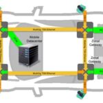
An example of an advanced application is an optical interface to a 100 GbE MAC (media access controller) with all support protocols including framing and forward error correction, Figure 1. Many FPGAs are used in much smaller, less sophisticated applications, where they combine various many logic functions and execute, in hardware circuitry, the functions and algorithms needed along with numeric processing.

As a hardware-based architecture, the FPGA is an attractive processing solution because it can simultaneously provide a user-selected balance among critical tradeoffs of high performance and speed, outstanding design-in flexibility including field programmability, and fast time-to-market. These are valuable attributes with today’s advanced products which must be developed, verified, and put into production on tight schedules. It also has lower non-recurring engineering (NRE) costs and is economical, even for low-volume products. Further, it allows assignment of most IC-package pins versus functions as desired, a big plus for PC-board physical layout.
In contrast to an FPGA, a conventional IC design is very costly in time and has high-risk factors. Any design defect or change in functions will result in a “re-spin” with major time delay and cost commitment. While in extremely high volumes, a conventional design using an ASIC (application-specific IC) – may be more cost- and power-effective, the time and risk factors will always remain. Other alternatives to the FPGA include the ASSP, SoC, and software-programmable device such as a μP or DSP. (see sidebar “If not an FPGA, then what?”)
Basic FPGA architecture and structure
Within the FPGA there are four major functions supporting logic resources and I/O resources: logic blocks and memory (RAM): configurable logic blocks (CLBs) consisting of registers (memory), muxes and combinatorial functional units (Figure 2). Some FPGAs also have a fifth function such as analog I/O.
The CLBs are embedded within a matrix array that contains routing which can be “programmed” to interconnect the CLBs. These CLBs exchange data using local and global interconnects, which are also programmable. The CLBs can implement Boolean-logic and combinatorial-logic via look-up tables (LUTs) which can then be combined with registers and muxes to become higher-level functions such as state machines or multipliers.

The RAM is used for writing, storing, and reading data, variables, and the many other transitory numbers with which any devices must deal. Some FPGAs provide much more than just the RAM; they also organize and include a memory controller to maximize memory-interface performance for off-chip memories.
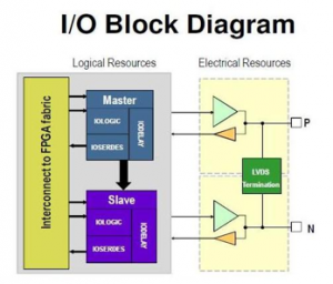
I/O blocks and digital inputs/outputs with programmable-parameters take the internal logic signals of the FPGA and match them to electrical requirements of the I/O ports (Figure 3). This includes providing the necessary input and output voltage thresholds, timing, slew rates, and drive for multiple I/O standards, among them LVCMOS (3.3 V, 2.5 V, 1.8 V, 1.5 V, and 1.2 V), LVPECL (3.3 V, 2.5 V), PCI, I2C, and LVDS.

Finally, there may also be some analog functionality. FPGAs are being used in a wider range of applications, where their virtues make them attractive technical and market alternatives to fixed-function ICs and software-based microcontrollers. In many of these roles, some basic analog input/output is involved, so an A/D or D/A converter may be part of the overall system. While FPGAs cannot match the performance of a high-end, stand-alone converter, they can provide a conversion function for many basic analog signals.
Choosing an FPGA
There are thousands of distinct FPGAs to consider; even if focused on a single vendor, there is still a long list of possibilities with various tradeoffs. The primary factors to consider are density, speed, I/O, power dissipation and rails, clocks and package size.
Density is a factor as designers don’t want to overspecify and thus pay for more FPGA gates than needed, but also want to allow some “insurance” in case the project needs to expand beyond the original estimate, or want to use the same FPGA across multiple end products. Speed is a parameter which indicates if the FPGA can support the logic needs of the task within the required time.
I/O count, of course, must be matched to the application. Some designs need only a few low-speed I/O ports, others need many ports, and some, such as software-defined radio (SDR) need serial I/O ports to support data streaming at several Gb/sec to and from the SDR A/D and D/A converters.
Power is always a concern, whether for sizing the system supply, accounting for thermal consideration, meeting regulatory requirements, or other reasons. While it is possible to specify the power it to a maximum, the reality is that the actual power dissipation depends on the FPGA’s final configuration, and operating modes. There are tools which can help quantify both average and maximum power needs. The DC power rails (there are usually multiple rails supporting the internal FPGA logic and the different I/O banks), must have sufficient output regulation to deal with transients in current demands.
As FPGA performance and speeds increase, so do the demands on the user-supplied external clocks. The latest generation of high-speed FPGAs has very tight frequency, timing and jitter requirements, as these clocks support the internal logic blocks; to manage propagation delays and skew, the clock must be near-perfect when it reaches the FPGA. Any deviations will have a ripple effect on FPGA timing and will adversely affect FPGA performance and integrity. FPGAs have clock buffers and related functions to internally distribute the clocks, and the programmed arrangement of these and the resultant clock-tree topology is a factor in ensuring specified performance.
Tools, libraries, and cores
It’s obviously not practical to manually decide how to connect the tens or hundreds of thousands of logic elements on an FPGA. Both FPGA vendors and independent third parties offer solutions.
Designers can use a structural view to describe the desired internal implementation, roughly analogous to providing a block diagram. Alternatively, they can use a behavioral view where they treat the system as a black box, and describe overall functionalities and I/O behavior desired. A hardware description language (HDL) then generates a netlist, which is a full description of logical ports and their connections.
Even this HDL approach would be too time-consuming and error-prone for a complex design with sophisticated algorithms. For these reasons, third-party vendors such as The Mathworks offer tools which translate high-level functions, simulations, and state diagrams into HDL code. As a result, a design can be drawn as a set of interconnected blocks at a very high level, its performance analyzed, and then translated into HDL code and then the netlist. Many FPGA and third-part vendors also offer large libraries of pre-defined, tested, and verified blocks for popular functions such as handling the data stream between the FPGA and high-speed converter, or analyzing data using standard criteria.
The full FPGA programming sequence involves many more steps and details, see sidebar “Simplified FPGA design flow”. There are many factors which must be evaluated after defining physical placement and routing, such as the critical path, timing closure, and performance simulation. (The critical path is the one with longest propagation delay through the FPGA; if its end-to-end delay is too long, the logic circuits will not perform to the designer’s specification).
Conclusion
The FPGA is a rare device in electronics, in that it has many strong virtues, and few (if any) drawbacks with respect to the application. For these reasons, it has become the digital processor of choice in many situations. By selecting an FPGA matched to the design, it is possible to have performance, low power, and low cost (due to efficient use of the die’s gates) along with relative ease of embedding high-level designs and algorithms, yet with no line-by-line coding. All this comes with the benefits of field programmability, which means the design can be tested, debugged, and easily changed, without a high NRE or time lag— even if requirements change or were misunderstood.
More FPGA-related content at www.avnet.com
______________________________________________________________________________________________________________________________________
Sidebars:
“If not an FPGA, then what?”
In addition to the ASIC, there are other alternatives to the FPGA. A standard available ASSP IC — an application-specific standard product) may be somewhat suitable, but it will likely need a significant amount of support circuitry and be a relatively costly solution in terms of footprint, power, time to market, and BOM cost, while lacking the flexibility of the FPGA. Similarly, a system on chip (SoC) which combines existing IC blocks into a larger die may be feasible, but has many of the weaknesses of the ASSP.
Finally, a standard microprocessor or digital signal processor (DSP) can be used, executing code stored in memory. While this provides the ultimate in flexibility and reprogrammability, it lacks the speed of hardware-only FPGAs. It does, however, easily support major changes in design algorithms or topologies, since it is entirely driven by the lines of code which can be re-written almost “on the fly”, downloaded, and tested.
Simplified FPGA design flow
In the simplified representation of FPGA design flow, Figure SB-1, each box, has many details, of course, but there is a logical flow to the steps. The BIT file near the end is the final set of instructions for how the FPGA gates are to be physically programmed using IC processes which are an outgrowth of PROM (programmable read only memory) technologies.

The configured FPGA has a final moment of truth: it has to be tested in a real circuit board, using appropriate test vectors, suites, or standards for the project. If the performance falls short, the FPGA high-level code-development tools with their simulation and evaluation modes, plus the JTAG hardware-interface port on many FPGAs, can then be used to investigate the shortfall.
About the author:
 Bill Schweber is an electronics engineer who has written three textbooks on electronic communications systems, as well as hundreds of technical articles, opinion columns, and product features. In past roles, he worked as a technical web-site manager for multiple topic-specific sites for EE Times, as well as both the Executive Editor and Analog Editor at EDN.
He has an MSEE (Univ. of Mass) and BSEE (Columbia Univ.), is a Registered Professional Engineer, and holds an Advanced Class amateur radio license. Bill has also planned, written, and presented on-line courses on a variety of engineering topics, including MOSFET basics, ADC selection, and driving LEDs


Leave a Reply
You must be logged in to post a comment.