Because it is able to function in so many diverse ways, the op-amp can be the defining element in electronic circuits of any complexity. Applications go far beyond amplification. Because they are near-perfect dc amplifiers, op-amps are suitable for filtering, signal conditioning, and for performing such mathematical operations as addition, subtraction, differentiation, and integration.
 Op amps have virtually infinite input impedance, meaning the current flowing into their inputs is vanishingly close to zero. The device looks at the voltage on these pins and then decides what to do in regard to the single output terminal, which has essentially zero output impedance.
Taking note of the difference in signal voltage present at the input terminals, the op-amp multiplies it by whatever gain is intrinsic to the specific device. A characteristic of the op-amp is that this gain, when the device is in open-loop configuration, is astonishingly high, as much as a million. This parameter is substantially reduced when the device is used in closed-loop configuration with negative feedback. Still, with such high gain in the first place, there is a lot of room for both negative feedback and gain.
When an op-amp is externally connected in a negative feedback configuration, there will always be two simple principles that apply:
•The output will react to the voltage difference between the two inputs to make it zero. It is important to realize that the actual voltage at the inputs is not affected. What happens is that the device takes note of the voltage states at the inputs and then adjusts the output terminal so as to make the external network endeavor to move the voltage difference at the inputs to zero.
•The inputs, with infinite impedance, draw no current.
Of the two high-impedance inputs, one is known as the inverting terminal, marked with a minus sign, and the other the non-inverting terminal, marked with a plus sign. It is important to realize that these pins are not necessarily positive or negative with respect to one another in the manner of power supply pins. The signs denote only which is inverting (-) and which is non-inverting (+) as they relate to the (usually) single output.
The output terminal can sink or source voltage or current. The output signal is equal to the input signal times the gain. There are four possible operating modes, depending upon input and output status:
• Voltage, when input and output voltages vary. This is by far the most common operating mode.
• Current, when input and output currents vary.
• Transconductance, when input voltage and output current vary.
• Transresistance, when input current and output voltage vary.
Some of the common op-amp applications are:
• As a buffer: Between circuits or stages an op-amp can be inserted as a voltage follower so as to perform a buffing function with unity gain. There is no signal inversion or amplification. The sole purpose is to provide isolation and prevent circuit loading. In this configuration, the output is connected directly back to an input so Vin = Vout. If there were a resistor or any sort of impedance in this line, the gain would go high and the circuit would not operate as a buffer.
• As an inverter: When the + input is connected to ground and the – input is connected to the midpoint of a resistive voltage divider whose endpoints are at Vin and Vout. This circuit inverts the signal but does not amplify it, which is to say gain = 1 when the two resistors are equal.
• As a non-inverting amplifier: When the output signal is connected to the non-inverting (+) input and the inverting input is connected to the midpoint of a resistive voltage divider that runs from ground to the output. There is amplification without inversion.
• As an inverting amplifier: When the + input is grounded and the – input is connected to the midpoint of a similar voltage divider.
• As a bridge amplifier: In this interesting circuit, inverting and non-inverting amplifier circuits join to form a bridge amplifier. The two outputs are connected to a load resistor.
In an ideal open-loop op-amp the gain is infinite, but there is always some intrinsic internal feedback, so this infinite level never actually happens. The real-world amount is likely to be either side of 100,000. Nevertheless, this is astronomical relative to the world of transistors.
Input impedance of an op-amp is also infinite, but this parameter is modified by input leakage current, sometimes in the milliamp range. This high figure is sufficient to prevent loading of the preceding circuit, one of the great advantages of the op-amp.
Similarly, the low (ideal zero) output impedance throughout its infinite bandwidth translates to overall equipment stability and reliability.
Two important op-amp implementations are as a differentiator amplifier and an integrator amplifier. Differentiation is a mathematical operation where the dependent variable is directly proportional to the rate of change with respect to time of the independent variable. Adhering to this definition, if input is substituted for the independent variable and output is substituted for the dependent variable, we can build an electronic circuit that will simulate the mathematical operation described above – a differentiator constructed using an op-amp.
A parallel situation exists with respect to integration, a mathematical process realized electronically whereby the output responds to changes in the input over time. Integration can easily be demonstrated graphically by drawing a waveform as seen in an oscilloscope display in the time domain. Amplitude is represented relative to the Y-axis and time is represented relative to the X-axis. Integration is the process of measuring the area under the resulting curve. In so doing we find the product of amplitude and time.
An integrator circuit is similar to an op-amp inverting amplifier except that the purely resistive feedback element is replaced by a frequency-dependent impedance, i.e. a capacitor. Because integration is time dependent, the RC network that is in the negative feedback circuit creates the integrating function.
The differentiator amplifier is similar to the integrator amplifier except that the capacitance sits upstream from the inverting input. The op-amp differentiator is inherently unstable at high frequencies and it is subject to harmonics and noise emanating from the preceding stage.
If a sine wave is applied at the input of an op-amp based differentiator, the output will be a cosine wave. A square wave at the input yields spikes where the input transitions occur and a triangle wave manifests at the output as a rectangular wave.
 There are a variety of op amp parameters that are important. They include bias current, offset voltage and current, and the op amp transfer function. In particular, measurements of the op amp transfer function can be set up using an oscilloscope, waveform or arbitrary function generator, and a simple circuit. The AWG produces a triangle wave used as an input to the op amp under test (DUT) and to drive the horizontal scope deflection. The output of the DUT is fed to the scope’s vertical input.
The DUT is driven by a 16 Hz ± 2.5 mV triangular wave derived from a ±5-V output of the AWG by means of voltage divider resistors. Another op amp in the circuit functions both as a voltage follower and as an integrator. When S1 is closed, a voltage develops across the 0.1
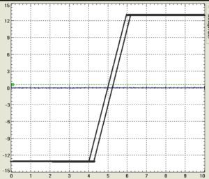
A typical transfer function for an op amp as traced out by the test circuit.
μF capacitor equal to the amplifier offset voltage multiplied by the gain of the feedback loop. When the switch opens, the charge stored on the capacitor continues to provide the offset voltage. The op amp also sums the triangular wave test signal with the offset correction voltage and applies this sum to the input of the DUT through an attenuating resistor network. This input sweeps the input of the DUT ± 2.5 mV around its offset voltage.
The resulting scope display is a plot of Vin vs Vout and provides information about gain, gain linearity, and output swing. Gain displays as the slope ΔVout/ΔVin of the transfer function. Gain linearity is the change in slope of the Vout/Vin display as a function of output voltage. Such a display is useful in detecting crossover distortion in a Class B output stage. Output swing is measured as the vertical deflection of the transfer function at the horizontal extremes of the display.
The amplifier is connected as a non-inverting unity gain amplifier. The amp output drives the differential input resistors for the DUT. The amplifier provides two functions; to provide an offset voltage correction to the input of the DUT and to drive the input of the device under test with a ±2.5 mV triangular wave centered about the offset voltage.
There are a few other components in the circuit. A resistor and two are necessary to control the integrator function when no DUT is present or when the DUT is faulty. The resistor provides a dc feedback path in the absence of a DUT and resets the integrator
to zero. The two diodes clamp the input of the integrator to about ±0.7 V if the DUT is faulty.


Leave a Reply
You must be logged in to post a comment.