(Part 1 looked at the basic function and operation of the charge-pump switched-capacitor voltage doubler. This versatile topology has some additional interesting considerations and permutations.)
What about the capacitor?
When MOSFET switches are used, the capacitor is sometimes called a “flying capacitor.” This is a designation which is a holdover from early days of electronics, when a similar arrangement was used to sample a sensor voltage. The sensor output would charge a capacitor, and then the capacitor would be disconnected from the sensor and switched to a voltage-reading circuit. In effect, the capacitor would “fly” between the sensor and electronics, but there was no electrical path between two sides. (In the earliest days, that switch was mechanical, not electrical, and use of mechanical switches, usually reed relays, continued well into the electronic era, as mechanical switches offered multi-megaohm isolation which electronic switches could not achieve.)
These capacitors can be small-value ceramic devices, or larger electrolytic ones, depending on the amount of current, the energy-storage needed, and the switching speed. The interplay among these parameters is also determined by the amount of output current to be charged into, and discharged from, the capacitors.
What else can a charge pump do?
While the basic arrangement provides voltage doubling, it is possible to instead convert a positive voltage to negative one, or vice versa, by clever rearrangement of the components, Figure. Further, if more switch and capacitor segments are added, the output voltage can be triple or quadruple the input (and go even higher). For this reason, charge pumps are sometimes called voltage multipliers. Still another arrangement allows the charge pump to act as a voltage “halver” or “divider.”
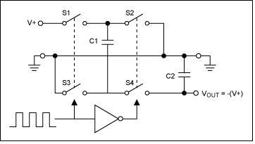
Figure 1: This reconfiguring of the basic boost-converter charge pump results in a circuit which converts a positive rail to a negative one, which is frequently needed for biasing or providing an offset voltage . (Source: Maxim Integrated)
What are the clock considerations?
The charge-pump clock generally operates in the 10-kHz to 2-MHz range; some clocks are now reaching 4 MHz. Use of a higher frequency minimizes the amount of capacitance required, as less charge needs to be stored and then dumped due to a shorter time cycle. However, there are higher losses and other negatives associated with switching at higher frequency, so there’s a tradeoff to be made.
Some charge pumps use a clock with low or moderate accuracy and stability (even the low-cost 555 timer can be used) and yield looser regulation specifications; while others use a more precise, fully controllable clock for more consistent performance and other benefits. Charge pumps are available with no need for an external clock – the user supplies it – as well as with embedded clocks for lowest parts count. The choice is made based on output regulation needs, system-level tradeoffs, BOM concerns, and cost.
How is filtering and regulation accomplished?
The pulsing nature of the higher-voltage output is smoothed by adding an output capacitor plus other components, in a standard filtering approach. While this does reduce output ripple, it does little to maintain output regulation as the load varies – yet regulation is one of the key parameters of a DC rail. Their output voltage is somewhat load dependent; higher loads result in lower average voltages.
The charge-pump solution to the regulation challenge is simple and elegant. By adjusting the duty cycle of the clock and thus the ratio of the two parts of the charge/discharge cycle, the output voltage can be closely regulated. This clock adjustment is dynamically controlled by a feedback loop from the output. A well-designed charge-pump with clock control can maintain regulation to within about 1%, which is more than sufficient for most applications; charge pumps with tighter regulation can also be available using with some additional design techniques.
Are charge pumps for every buck or boost situation?
No. Charge pumps are very effective solutions for lower-current ranges of under about 100 to 500 mA, and they are best when the design needs just a small amount of current at a voltage that is not already available, or locally regulated rail is needed for best performance. However, they are not a good choice at higher current levels.
With some additional circuitry, switches, and more-involved architecture, they can implement a merged buck/boost regulator design with seamless transition between modes. For example, this boost/buck mode is needed where output of a Li-ion battery can range from 3.6 V when fully charged, down to 1.5 V when drained, yet the output must be maintained at 3.0 V. The combined buck boost converter starts in buck mode, then transitions to boost mode as the battery drops below the 3.0 V level; all the while, the converter output is a steady, glitch-free rail.
What about embedded charge pumps?
Charge-pump designs are available as standalone ICs which can be used to provide power rails for ICs, or just to develop low-current bias voltages for displays, among other applications. Charge-pump functionality can also be embedded within ICs, rather just be offered as separate devices.
For example, an RS-232 IC may need only a low voltage such as 3 V or 5 V for its internal functions, but also needs a higher DC voltage of 12 V to meet the interface standard’s requirements. Rather than supplying two distinct rails to the RS-232 IC, a single low-voltage rail is used and it is boosted by an internal charge pump within the RS-232 IC to the higher voltage for the I/O interface. The same technique is used in many large-scale digital ICs which use a low voltage internally, but need a higher voltage for their many interface and I/O pins.