PAM4 modulation boosts throughput but adds test challenges.
Part 1 of this two-part series described the evolution of the PCI Express (PCIe) standard, including the move from non-return-to-zero (NRZ) signaling in PCIe 5 to four-level pulse-amplitude modulation (PAM4) signaling in PCIe 6.
What unique test challenges does PCIe 6 present?
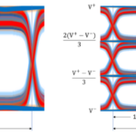
As mentioned in Part 1, PAM4 signaling stacks three eyes vertically in each unit interval (UI), as shown in Figure 1 on the right. Consequently, the eye height for a PCIe 6 PAM4 signal is one-third that of a PCIe 5 NRZ signal (Figure 1, left), resulting in a degradation of signal-to-noise ratio (SNR) of 20log10(1/3) = -9.54 dB.

The reduced SNR makes PCIe 6 implementations susceptible to errors resulting from the power supply and other noise sources. Whereas DSP-based equalization schemes can compensate for some impairments, some nonlinear errors in a PCIe 6 link cannot be compensated for. To help quantify errors that can and cannot be compensated for, the PCIe Special Interest Group (PCI-SIG) uses the signal-to-noise-and-distortion ratio in dB:

Here, pmax equals a pulse’s peak power, σn equals the standard deviation of the noise in the pulse response, and σe equals the standard deviation of the nonlinear distortion.
What do I need to measure those parameters?
To measure these parameters on a transmitter under test, you’ll need a real-time oscilloscope with a bandwidth of 50 GHz, PCIe 6 post-processing software, and a new set of compliance patterns for PCIe 6. The compliance patterns include pseudorandom bit sequences (PRBSs) as well as long (64-UI) strings of 0s, 1s, 2s, and 3s.
How do I proceed?
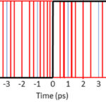
To measure σn, configure your transmitter under test to generate strings of 64-UI 0s, 1s, 2s, and 3s. Figure 2 shows a 64-UI string of 1s. Zoom in on the 61st UI — by then the noise will have stabilized, and you can proceed much as you would for a traditional DC SNR measurement. Take evenly spaced samples of the 61st UI voltage and calculate the RMS noise level.

To measure pmax, configure your transmitter to generate a PRBS and use the oscilloscope to capture each output pulse. Post-processing software will perform a linear-fit operation, based on IEEE methodology, relating the captured pmax to the ideal response, allowing the software to extract the nonlinear contributions, which make up the distortion σe. You will also need to account for the oscilloscope’s contribution to the total noise and distortion. In a blog post, Teledyne LeCroy presents an alternative form of the SDNR equation that accounts for the oscilloscope. In a white paper, Cadence advises using a fourth-order Bessel-Thomson filter with a -3 dB cutoff frequency at 33 GHz to limit oscilloscope noise contribution.
What other measurements are unique to PCIe 6?
With PAM4, the four voltage levels must be evenly spaced. To quantify improper spacing, PCIe 6 introduces the ratio of level mismatch (RLM). To measure transmitter RLM, you evaluate three expressions based on measurements of V0¬, V1, V2, and V3 and the calculated VMID, the midpoint between V0¬ and V3¬:
3(V1–VMID)/(V0–VMID)
3(V2-VMID)/(V3–VMID)
2-3(V1–VMID)/(V0–VMID)
2-3(V2–VMID)/(V3–VMID)
Make the voltage measurements using the same 64-UI strings used to measure σn. RLM is the minimum of the four expressions. Ideally, they will all equal 1, and your RLM will be 1. If any are less than 1, then at least one of your PAM4 eye heights will be even less than one-third of the NRZ eye height, an impairment that will increase errors. A white paper coauthored by Tektronix and Synopsys has more.
How does the PCIe 6 standard address the higher error rates associated with PAM4?
PCIe 6 employs a forward error-correction (FEC) function and a cyclical redundancy check (CRC) and retry mechanism. The Cadence white paper has more details. In addition, as mentioned in part 1, PCIe 6 uses Gray coding to reduce bit errors and facilitate error correction. Table 1 illustrates how Gray coding helps. Suppose a transmitter transmits a decimal 2 (V2) but because of channel impairments the transmitted signal falls below the level 2 threshold voltage and is received as a 1. With binary code, that results in two bit errors, but with Gray code, only one bit error.
| Transmitted Decimal Number |
Transmitted binary code | Received Binary Code* |
Received Decimal Number | Bit errors |
| 2 | 1 0 |
0 1 |
1 | 2 |
| Transmitted decimal number | Transmitted Gray Code | Received Gray Code | Received decimal number | Bit errors |
| 2 | 1 1 |
0 1 |
1 | 1 |
| *Bit errors shown in red. |
Table 1. Bit Errors for Binary vs. Gray Code.
What other tests are required for PCIe 6?
There are many additional tests. Keysight has a solution brief citing the various aspects of PCIe 6 design and test, including physical-layer system simulation, physical-layer interconnect design, physical-layer transmitter and receiver test, and protocol-layer test.
What’s next for PCIe?
The PCI-SIG plans to introduce PCIe 7 in 2025. It will use PAM4 signaling to deliver a 128-GT/sec raw bit rate. It will transfer up to 512 GB/s bi-directionally in a x16 configuration. The PCI-SIG said that it will continue focusing on low latency, high reliability, improved power efficiency, and optimized channel parameters and reach — that is, the length of the PCIe physical connection between two devices. PCI-SIG expects PCIe 7 to find use in 800G Ethernet, artificial intelligence and machine learning, cloud and quantum computing, and military/aerospace applications.