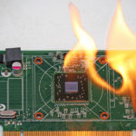
When designing any electronics that consume a significant amount of power, you need to consider where that power will go. With power electronics –such as IGBTs, power FETs, or power transistors – you might be expecting most of it to end up in your load, but there will be some which don’t. Even devices that are not considered “power devices” need to have their power consumption checked – high-speed devices such as analog-to-digital converters (ADCs) and op amps can consume significant amounts of power. That power is not usually going into a load, so most will be dissipated in the device. Factor in that devices are getting smaller, so thermal resistance increases and the problem becomes worse.
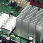
Thermal resistance is usually quoted as a temperature rise (°C) per Watt of power. The temperature rise is between two points and under certain specified conditions. One of the two points is often the semiconductor device junction. The other point could be the ambient air, but it is more often the “case” of the device. However, with the devices becoming more sophisticated to dissipate power better, the “case” can be the “case while soldered to a certain area of PCB”. T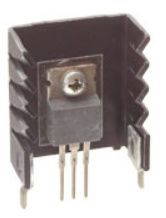 his is because the PCB is acting as a heatsink, whereas with traditional power devices such as TO220 packages, the heatsink is often a metal extrusion or pressing bolted or clipped to the device such as this one from Aavid Thermalloy (left)
These types of heatsinks are simple to select. They are specified with the thermal resistance from the device to the air, such as 13°C/W. Once you know the device’s thermal resistance from junction to case, say 4°C/W, you can add these together, work out your total temperature rise, and see if you are still within the device’s maximum junction temperature. You are more likely to be doing the calculation the opposite way round – deciding on the maximum temperature rise you can allow and then calculating the smallest heatsink that will keep you within that.
Bear in mind that the “ambient” temperature is not necessarily the temperature of the equipment surroundings but the ambient air around the heatsink. If the equipment is in an enclosure, then the temperature inside the enclosure can be a lot higher than the ambient air outside the enclosure. Also, the orientation of heatsinks makes a difference, i.e., vertical or horizontal. A standard heatsink will usually specify which orientation the thermal resistance is quoted for.
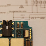
Newer surface mount power devices are a somewhat more complex problem. The devices are smaller, and to better dissipate power; newer packaging solutions often put a pad under the device to remove heat from the silicon. While they can look the same on the outside, on the inside, they can be different, resulting in better or worse thermal conductivity to the heatsink pad. Texas Instruments has its trademarked PowerPAD construction, and a comparison of where the heat goes is in its 1998 SMI Conference presentation, which can be downloaded as a pdf.
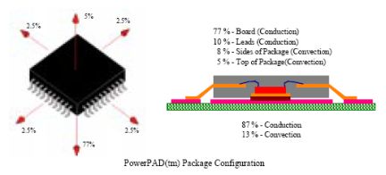 Whereas a conventional package would conduct 80% of the heat through the legs, the PowerPAD construction would dissipate 77% through the board through the PowerPAD rather than through the legs. Many small packages are designed to dissipate power through the PCB, either through the legs, a power tab, or a power pad, but they all have one thing in common – the PCB is your heatsink. The problem with that is the difficulty in being sure of the thermal resistance from the device junction to the ambient air. You will find some guidance in datasheets.
For example, the Linear Technology (now Analog Devices) LT1763 regulator has a table (below) for each device package giving thermal resistances depending on the board area used for dissipating the heat.
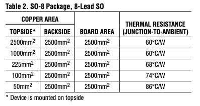
In all cases, they rely on 2,500 mm2 of area dissipating heat on the underside of the PCB with varying amounts of the topside area also used for heat dissipation. It is unlikely that you would dedicate 2,500 mm2 to heatsinking on both sides of the PCB. Also, it is somewhat ironic that while trying to make devices smaller and smaller, you now need to allow 200 times the area of the device as a PCB heatsink to keep it cool! Hopefully, the space will not be dedicated to being a heatsink but will be a ground plane under other circuitry.
 You will also find more complex examples where a four-layer board is assumed, and inner layers are used for dissipation. Also, vias in power pads are usually used to conduct heat to the inner or bottom PCB layers. Again, these would normally be specified on the datasheet, so you know the assumptions in the quoted thermal resistance figures.
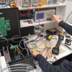
Ultimately, the only way to be sure is to build something and test it using a thermal camera or another method to determine device temperature. If you have a large margin in your power calculations, then testing will not be critical.
Another way of dissipating power is to use a metal-backed or metal-cored PCB. These are usually only single or dual-layer PCBs, and they are generally reserved for specific power applications such as high-power LED mounting. However, you can metal back multilayer PCBs.
Using Alumina rather than fiberglass (FR4) for a PCB would help dissipate heat because Alumina has 100 times the thermal conductivity of FR4. However, it is instead a specialized solution.
Don’t neglect the benefits of air movement. Any airflow over the PCB reduces the temperature rise, which is why fans are used in equipment. Standard heatsinks often give a graph of effective thermal resistance against airflow.
Even water cooling is possible. I worked on a project which was heating and pumping water. The heater’s power device was mounted, so it was thermally connected to the cold water flow. This had a double benefit as it kept the power device cool, but also the heat wasn’t wasted – it preheated the water, which was due to be heated anyway.

Leave a Reply
You must be logged in to post a comment.