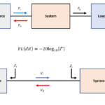
Part 1 looked at impedance matching and the need for a complex conjugate impedance at the load, compared to the source impedance. Once the need for an impedance-matching network is determined — and it is very likely needed — the next challenge is defining and creating this network. It may seem that doing a few calculations using a software package is all that is needed, but the reality is far more complicated. The Smith chart is a very helpful graphical tool for developing the matching network.
Q: What are the challenges in impedance matching?
A: The first challenge is figuring out what the source output impedance and load impedance actually are. In some cases, such as individual components, the vendor provides this data; however, parasitics and other in-circuit factors will change these values. In many cases, impedances must be determined by a detailed model of the circuit and its many elements, which is a difficult task for high-frequency RF. In these cases, impedances must be measured. The difficulty of assessing these impedances increases with frequency.
Q: How are these impedances measured?
A: A sophisticated test instrument called a vector network analyzer (VNA), as well as a test suite are used (Figure 1.) The VNA sweeps across the frequency range of interest, measures the impedance, and then provides a table or graphical representation of the results.

Q: Once you know the source and load impedance, what’s the next step?
A: The next step is to devise a matching network so that the source sees an impedance equal to its complex conjugate, and the load sees a source with an impedance equal to its own complex conjugate. There are many topologies for implementing networks that can do this, but determining the specific values of the components within these networks is very difficult.
Q: Why is this difficult? Isn’t this just a matter of detailed calculations which can be automated?
A: Yes and no. Certainly, the component values can be worked out for a given matching-circuit topology. But the choice of “best” topology among the possible ones is a function of design priorities. Consider an analogy: you need to travel from point A (the source impedance) to point B (the load impedance). Do you take the fastest route, the shortest route, the one that is most scenic, the cheapest route, the one you have traveled before and with which you are comfortable, or one where you can stop along the way and see some sites?
It’s the same with determining the path from A to B for the matching network; it’s not just a simple matter of observing the closest-fit curved path between the two points. You can focus on the fewest components, the smallest overall footprint, the lowest cost, parts that are already on the BOM (bill of materials), component trimmability, or the path which is most tolerant of component variations and temperature coefficient, among many design considerations. In other words, there is no single “optimum” choice; instead, it depends on many conflicting factors.
Q: What tools can be used facilitate determining the matching component options?
A: A graphical tool called the Smith chart, named after its creator Phillip Smith, is most commonly used. This tool was developed by Smith in the 1920s when he was working on VSWR measurements and understanding the basics transmission lines at Bell Telephone Laboratories, see Reference 1.
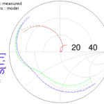
A greatly simplified version of the chart (Figure 2), shows how it uses non-concentric curves to represent resistance, capacitance, and inductance, so any complex impedance can be plotted on the chart. While the use of the Smith chart is complicated and beyond this FAQ, it allows the user to plot the source and load impedances, and then see all the possible paths between them, see References.

In brief, the detailed chart, Figure 3, guides the selection of component types (L, R, C) and values which will take the impedance on the various paths that are possible. The design engineer looks at the components required to travel each path (their type, value, and quantity) and decides which set makes the most sense with respect to the system priorities.

Q: Isn’t a chart somewhat antiquated?
A: Yes, the paper version of the Smith chart is largely obsolete. But the usefulness of this tool is proven by the fact that many test instruments, including the VNA, plot the results on a Smith chart on their screen. This allows the user to see the results, make adjustments and changes, and see the impact of these changes.
References
- EDN, “The Smith chart: more vital after all these years”
- RF Café, “IEEE MTT-S Buys Rights to Smith Chart”
- Engineering and Technology Wiki, “Smith Chart”
- Maxim Integrated, Tutorial 742, “Impedance Matching and the Smith Chart: The Fundamentals”
- National Instruments, “Impedance and Impedance Matching”
- University of Kansas, EECs Dept., “Chapter 5 – Impedance Matching and Tuning”
- San Jose State University, “Impedance Matching and Matching Networks”
- Keysight Technologies, Smith Chart format


Leave a Reply
You must be logged in to post a comment.